

VDMOS device
A device and channel technology, applied in the field of semiconductor power devices, can solve problems such as difficult manufacturing process, limited application, poor dynamic characteristics of body diodes, etc.
- Summary
- Abstract
- Description
- Claims
- Application Information
AI Technical Summary
Problems solved by technology
Method used
Image

Examples
Embodiment Construction
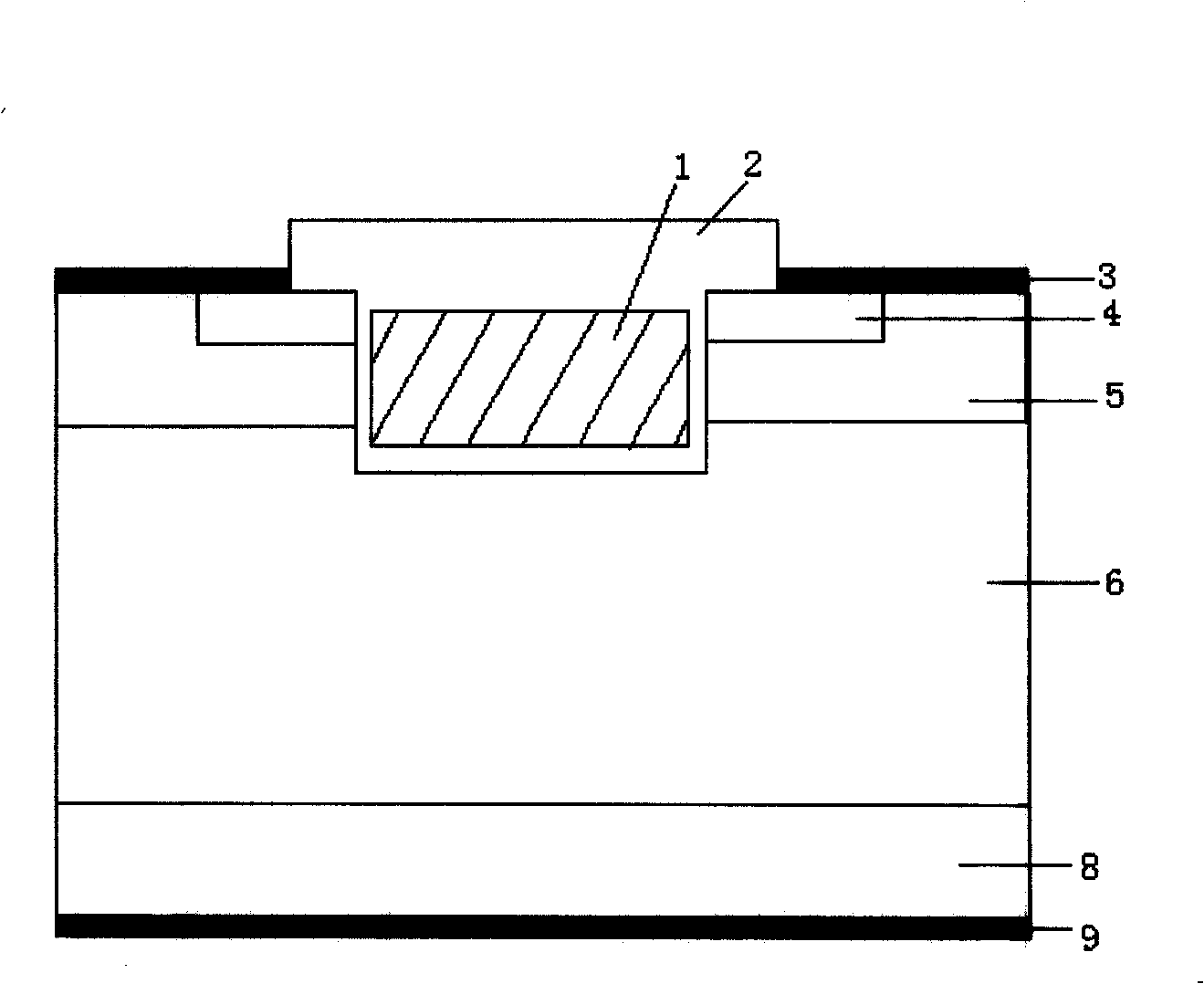
[0026] Taking the N-channel VDMOS device provided by the present invention as an example, the specific implementation manner of the present invention will be further described. Using the present invention to introduce a N under the P-type base region +The VDMOS structure of the first layer can obtain a lower conduction voltage drop, and achieve a better compromise between the forward conduction voltage drop and reverse recovery characteristics of the VDMOS inherent body diode, and the process is less difficult and more operable.
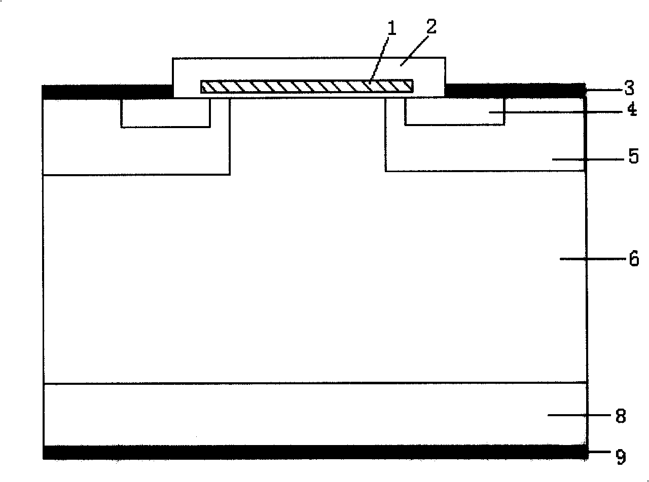
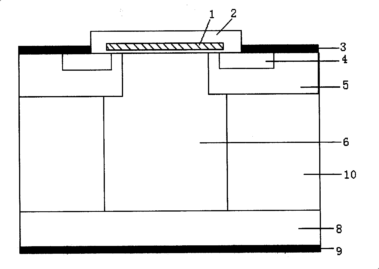
[0027] Introduce-N + layer VDMOS structure, such as Figure 4 As shown, including polysilicon gate 1, isolation dielectric 2, source metal 3, N + Source region 4, P-type base region 5, N - Drift zone 6, N + Layer 7, N + Substrate 8, drain metal 9.
[0028] During specific implementation, its main manufacturing steps include: (1) in N + N grown on silicon - Epitaxial layer, photolithography and phosphorus implantation, continue to grow N - Ep...
PUM
 Abstract
Description
Claims
Application Information