

III nitride compound semiconductor laminated structure
A stacked structure and nitride technology, which is applied in semiconductor devices, semiconductor/solid-state device manufacturing, coatings, etc., can solve problems such as unrecorded formation, and achieve the effect of improving production efficiency
- Summary
- Abstract
- Description
- Claims
- Application Information
AI Technical Summary
Problems solved by technology
Method used
Image

Examples
Embodiment 1
[0096] In this example, on the c-plane sapphire substrate, a layer made of AlN containing columnar crystals with clear grain boundaries was formed by RF sputtering as the first layer, and on the first layer, as the second layer was formed by MOCVD A layer formed of GaN.
[0097] First, only one side of the c-plane sapphire substrate is mirror-polished to the extent that it can be used for epitaxial growth, and it is introduced into a sputtering machine without any special wet pretreatment. The sputtering machine used has a high-frequency power supply and a mechanism capable of moving the position of the magnet within the target.
[0098] Initially, the substrate was heated to 750°C in the sputtering device, nitrogen gas was introduced at a flow rate of 15 sccm, the pressure in the chamber was maintained at 0.08 Pa, and a high-frequency bias voltage of 50 W was applied to the substrate side, by exposure to nitrogen plasma. Wash the substrate surface.
[0099] Next, after intr...
Embodiment 2
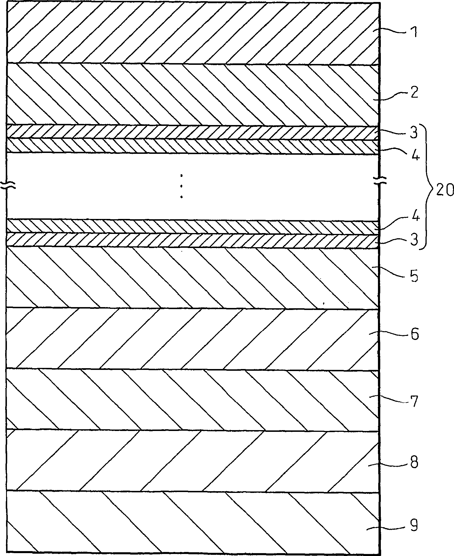
[0111] In this example, the manufacture of a group III nitride compound semiconductor light-emitting device using the group III nitride compound semiconductor stacked structure of the present invention will be described. In this example, using the same conditions as in Example 1, an n-type contact layer with Si as a dopant, etc. was formed on the non-doped GaN crystal (second layer) produced over 6 μm, and finally produced figure 1 The epitaxial wafer with the epitaxial layer structure for the shown semiconductor light-emitting element, that is, the epitaxial wafer has the following structure: on the sapphire substrate 9 with the c-plane, adopt the same growth method as the method described in Example 1 to form the epitaxial wafer containing On the AlN layer 8 (first layer) with a thickness of 50 nm and a columnar crystal structure with clear grain boundaries, the following layers are sequentially stacked from the substrate side: an undoped GaN layer 7 (second layer) with a thi...
Embodiment 3
[0123] In this embodiment, a rotating cathode RF sputtering method is used to form a layer of AlN containing columnar crystals with clear crystal interface on the sapphire c-plane substrate as the first layer, and a GaN layer is formed on the first layer by MOCVD As the second layer, the same epitaxial layer for LEDs as in Example 2 was formed on the second layer. The substrate temperature during sputtering was 700° C., and other conditions were the same as in Example 2.
[0124] As a result, after the epitaxial layer for LEDs was grown by the MOCVD method, the surface of the wafer taken out from the reactor was a mirror surface.
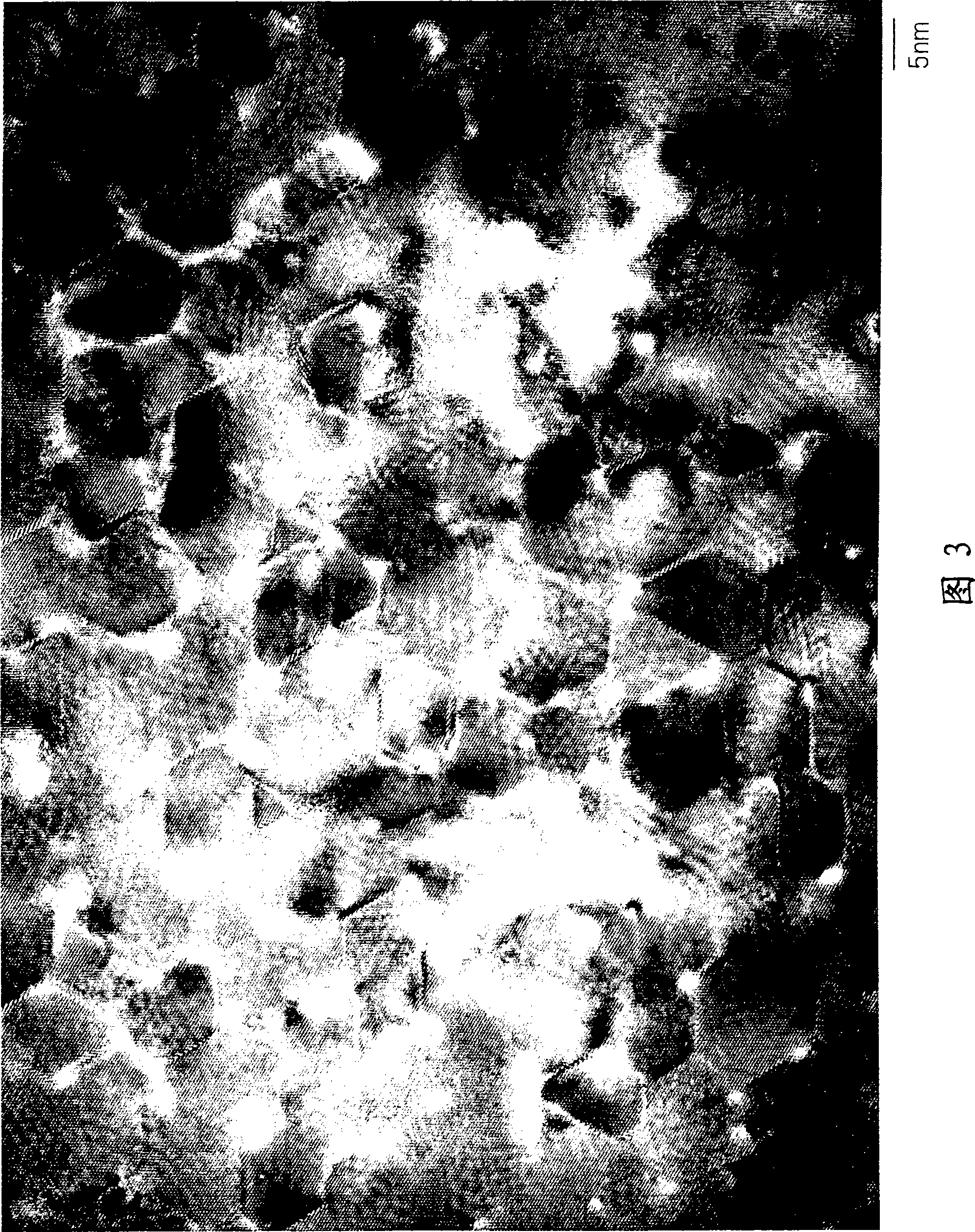
[0125] Using the same method as in Example 1 to observe the results of the first layer, the first layer formed of AlN formed by RF sputtering has a width of about 5 to 10 nm and a density of 5×10 crystals. 3 pieces / μm 2 Columnar crystals with clear crystal boundaries on the left and right.
[0126] The wafer manufactured as described above was us...
PUM
| Property | Measurement | Unit |
|---|---|---|
| width | aaaaa | aaaaa |
| width | aaaaa | aaaaa |
| thickness | aaaaa | aaaaa |
Abstract
Description
Claims
Application Information