Design method of multi-layer metal dielectric film capable of implementing imaging function

A multi-layer metal and design method technology, applied in optical components, optics, instruments, etc., can solve the problems of information not including evanescent wave components, resolution limit limitation, and inability to propagate outwards.

Active Publication Date: 2009-05-27
INST OF OPTICS & ELECTRONICS - CHINESE ACAD OF SCI
View PDF1 Cites 14 Cited by
  • Summary
  • Abstract
  • Description
  • Claims
  • Application Information

AI Technical Summary

Problems solved by technology

[0002] According to the Abbe-Rayleigh criterion, the resolution of the imaging system is strictly limited by the wavelength of the incident light and the numerical aperture. Theoretically, the resolution distance cannot be less than 1 / 2 wavelength. It can be used to observe the microstructure at a magnification of nearly a hundred times, but it is also limited by the resolution limit; this is because when the light is incident on the surface of the object, a part of the propagating wave component will interact with the surface of the object and propagate outward, but there is still Some evanescent wave components are bound on the surface of the object and cannot propagate outward. The information detected in the far field does not contain evanescent wave components, so the ability to resolve objects is limited, that is, the resolution limit. Therefore, research on systems beyond the diffraction limit resolution is in It is of great significance in scientific research, medicine, testing, etc.
[0003] Currently, there are several methods to achieve super-resolution imaging, scanning near-field optical microscopy (SNOM) (D.W.Pohl, D.Courjon, Near Field Optics, Kluwer, The Netherlands, 1993), near-field superlens (“Sub-Diffraction- Limited Optical Imaging with a Silver Superlens”; Nicholas Fang, HyesogLee, Cheng Sun, Xiang Zhang.Science 2005, 308, 534-537), etc. Near-field detection is to use probes to detect near-field evanescent wave information, record information and pass Data processing is used to restore the surface information of the object, but because the probe is scanned line by line, the scanning process is slow, which is not conducive to biological detection and other situations that need to respond to changes in the surface of the object in real time
Superlens uses a thin film structure to amplify and transmit the evanescent wave information localized on the surface of the object, but the structure has strict requirements on the dielectric constant of the metal and the medium in order to achieve the evanescent wave amplification effect, that is, its dielectric constant Must satisfy: ε m +ε d = 0; and the distance between the object and the image is very short when the superlens is used to zoom in, which is not conducive to the detection requirements in practical applications; in addition, the resolution of the suprelens is low

Method used


Image

  • Design method of multi-layer metal dielectric film capable of implementing imaging function
  • Design method of multi-layer metal dielectric film capable of implementing imaging function
  • Design method of multi-layer metal dielectric film capable of implementing imaging function

Examples


Embodiment 1

[0048] The concrete steps of embodiment 1 of the present invention are as follows:

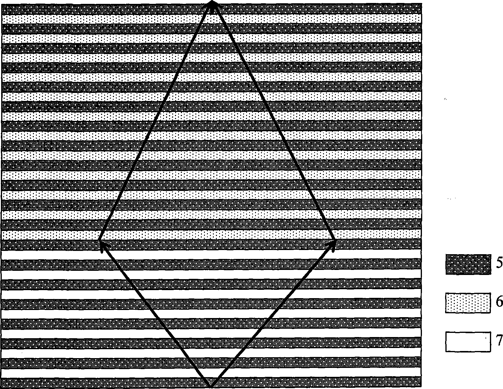
[0049] (1) Select the incident light wavelength to be 365nm, select the first group of materials to be metallic silver and air, and metallic silver has a refractive index of n under the irradiation of this wavelength Ag =0.039275+1.614224i ("Optical Constants of Noble metals".P.B.Johnson, R.W.ChristyP.R.B.1972), the corresponding dielectric constant ε 1 =—2.6042+0.1268i, the dielectric constant of air is ε 2 =1, take the thickness d of silver and air layer 1 , d 2 Both are 5nm, and the silver layer and the air layer are alternately arranged to construct the first multilayer film structure, then the real part of the equivalent dielectric constant of the silver-air multilayer film can be obtained by formula (1):

[0050] ε x1 =-0.8021,ε z1 =3.2467

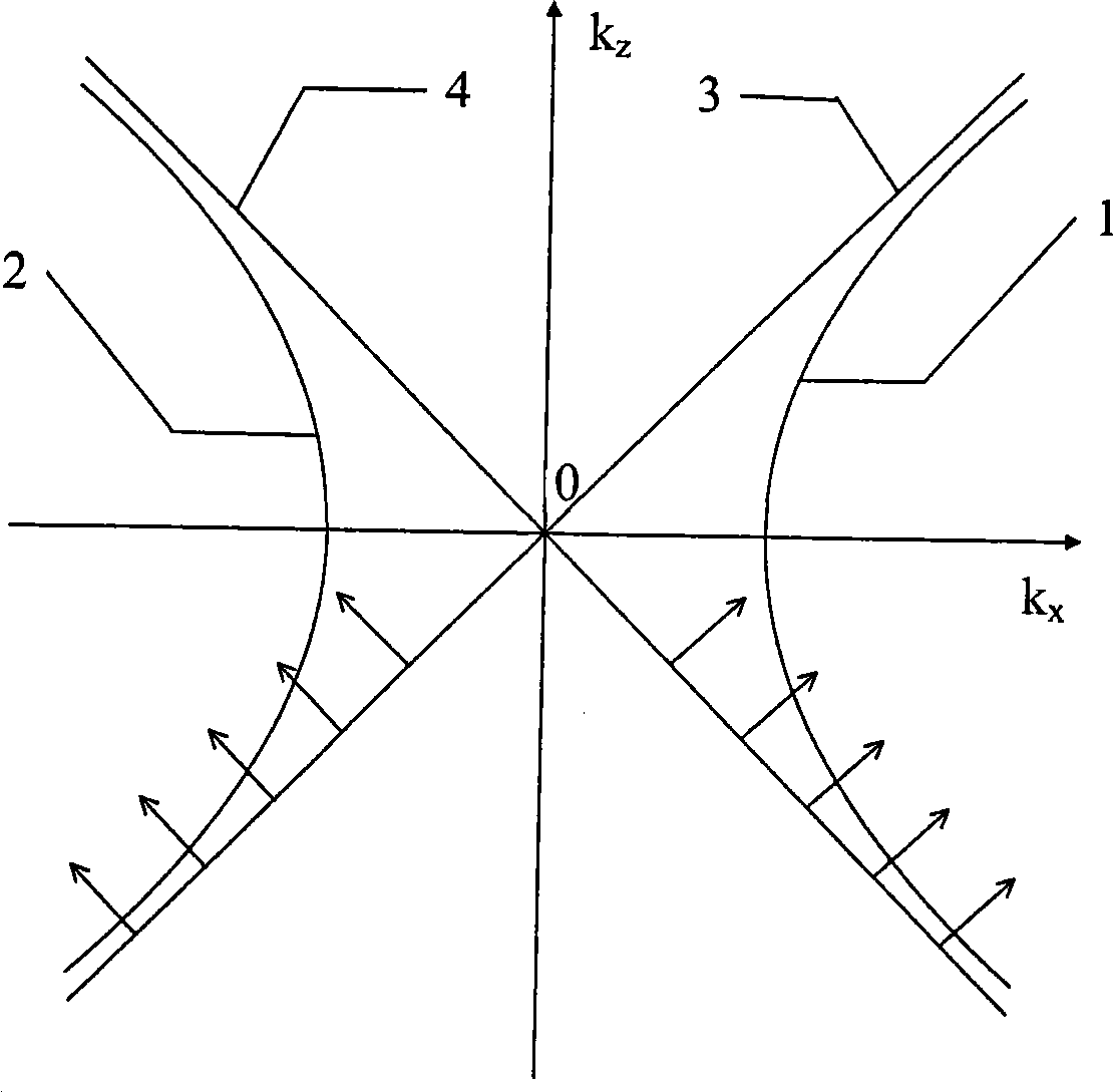
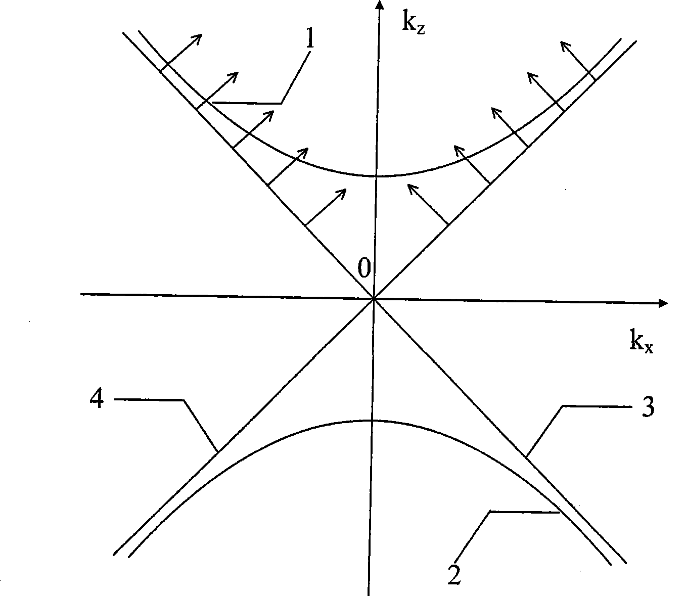
[0051] When the TM wave propagates in this kind of medium, k x and k z The equation corresponding to the functional relationship of is:

[...

Embodiment 2

[0069] The concrete steps of embodiment 2 of the present invention are as follows:

[0070] (1) The incident light wavelength is 365nm, and the first group of materials is selected as metal aluminum and silicon dioxide. Under the irradiation of this wavelength, the refractive index of metal aluminum is n Al =0.407+4.426i, the corresponding dielectric constant ε 1 =-19.4238+3.6028i, the refractive index of silicon dioxide n sio 2 = 1.45671 , The corresponding dielectric constant is ε 2 =1.45671 (the above parameters are taken from Handbook of OpticalMaterials, CRC Press), get the thickness d of aluminum and silicon dioxide layer 1 , d 2 Both are 10nm, and the first multilayer film structure is constructed by alternately arranging aluminum layers and silicon dioxide layers, then the real part of the equivalent dielectric constant of the aluminum-silicon dioxide multilayer f...


PUM

PropertyMeasurementUnit
thicknessaaaaaaaaaa
thicknessaaaaaaaaaa
thicknessaaaaaaaaaa

Abstract

A design method for multi-layer metal dielectric film capable of realizing the imaging function is characterized by selecting incident wave; selecting two sets of metallic material and dielectric material with a certain thickness, alternatively arranging the metal and medium in two sets to form two kinds of multi-layer metal dielectric film structures, respectively computing the equivalent dielectric constant of the two kinds of multi-layer metal dielectric film structures based on equivalent dielectric constant of each material and the thickness of each film layer; realizing the variation of the value and plusminus of the dielectric constant in respective direction by designing the thickness of each film layer so as to make the optical wave diverge through the first set of multi-layer metal dielectric film structure and converge through the second set of multi-layer metal dielectric film structure; binding the divergent structure multilayer film and the convergent structure multilayer film together according to a specific thickness ratio to the multi-layer metal dielectric film structure device which can make the fine structure far less than the operating wavelength image so as to achieve the super resolution.

Description

technical field [0001] The invention relates to a structure for super-resolution imaging using a heterojunction metal dielectric thin film, in particular to a design method for a multi-layer metal dielectric film capable of realizing the imaging function. Background technique [0002] According to the Abbe-Rayleigh criterion, the resolution of the imaging system is strictly limited by the wavelength of the incident light and the numerical aperture. Theoretically, the resolution distance cannot be less than 1 / 2 wavelength. To observe the microstructure at a magnification of nearly a hundred times, but it is also limited by the resolution limit; this is because when the light is incident on the surface of the object, a part of the propagating wave component will interact with the surface of the object and propagate outward, but there is still Some evanescent wave components are bound on the surface of the object and cannot propagate outward. The information detected in the far...

Claims


Application Information

Patent Timeline
Patent Type & Authority Applications(China)
IPC IPC(8): G02B27/00
Inventor 罗先刚赵延辉杜春雷王长涛
Owner INST OF OPTICS & ELECTRONICS - CHINESE ACAD OF SCI
Why Eureka
Try Eureka