

Method for preparing antapex contact crystalline silicon solar cell by utilizing passivation on double surfaces and laser dotting
A solar cell, double-sided passivation technology, applied in circuits, electrical components, semiconductor devices, etc., can solve the problems of high cost of magnetron sputtering, slow laser melting of A1 electrodes, and difficulty in large-scale production. Effects of rear recombination rate, open-circuit voltage and short-circuit current improvement, and conversion efficiency improvement
- Summary
- Abstract
- Description
- Claims
- Application Information
AI Technical Summary
Problems solved by technology
Method used
Image

Examples
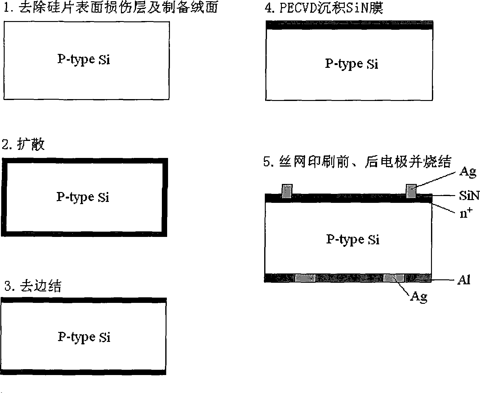
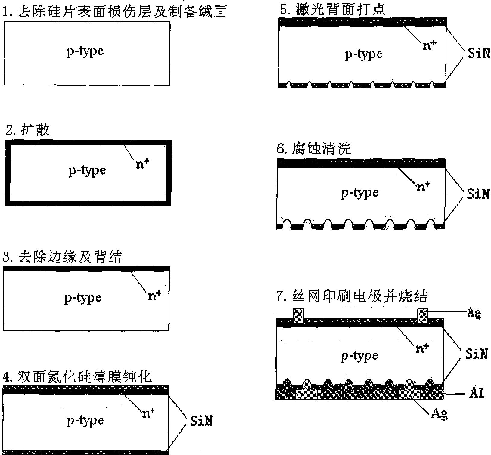
Embodiment 1
[0021] Such as image 3 As shown, a single-layer silicon nitride film is used for double-sided passivation, and the laser is quickly opened on the back to open the window, and then the electrode is prepared by screen printing. The process is as follows:
[0022] 1. Chemical etching removes the damaged layer on the surface of the silicon wafer, prepares the suede structure and performs pre-cleaning before diffusion.
[0023] 2. Phosphorus diffuses to form a p-n junction. For conventional tubular diffusion, silicon wafers are used back-to-back, in POCl 3 One-sided diffusion in atmosphere. For chain diffusion, the silicon wafer is sprayed with phosphorus source on one side, followed by rapid diffusion. But even for single-side doping, there will always be a part of the p-n junction on the back of the silicon wafer, which is due to the evaporation of the phosphorus source during the diffusion process.
[0024] 3. Remove edges and back knots. For back passivation and back ele...
Embodiment 2
[0030] Such as Figure 4As shown, a single-layer silicon nitride film is used for passivation and anti-reflection on the front surface, and a single-layer silicon nitride film, silicon oxide film, amorphous silicon film or microcrystalline silicon film can be used for rear surface passivation, and then the laser is used on the rear surface The window is quickly opened, and then the electrode is prepared by magnetron sputtering. The process is as follows:
[0031] 1. Chemical etching removes the damaged layer on the surface of the silicon wafer, prepares the suede structure and performs pre-cleaning before diffusion.
[0032] 2. Phosphorus diffuses to form a p-n junction.
[0033] 3. Remove edges and back knots.
[0034] 4. Perform double-sided passivation. The front surface adopts PECVD or PVD to deposit silicon nitride film for passivation and anti-reflection, and the back surface passivation adopts silicon nitride film, silicon oxide film, amorphous silicon film or micro...
Embodiment 3
[0040] Such as Figure 5 As shown, the double-sided double-layer passivation method is adopted. The front and rear surfaces of the silicon wafer are laminated with silicon nitride / silicon oxide films, and then the laser is quickly opened on the back to open the window, and then the electrode is prepared by screen printing. The process is as follows:
[0041] 1. Chemical etching removes the damaged layer on the surface of the silicon wafer, prepares the suede structure and performs pre-cleaning before diffusion.
[0042] 2. Phosphorus diffuses to form a p-n junction.
[0043] 3. Remove edges and back knots.
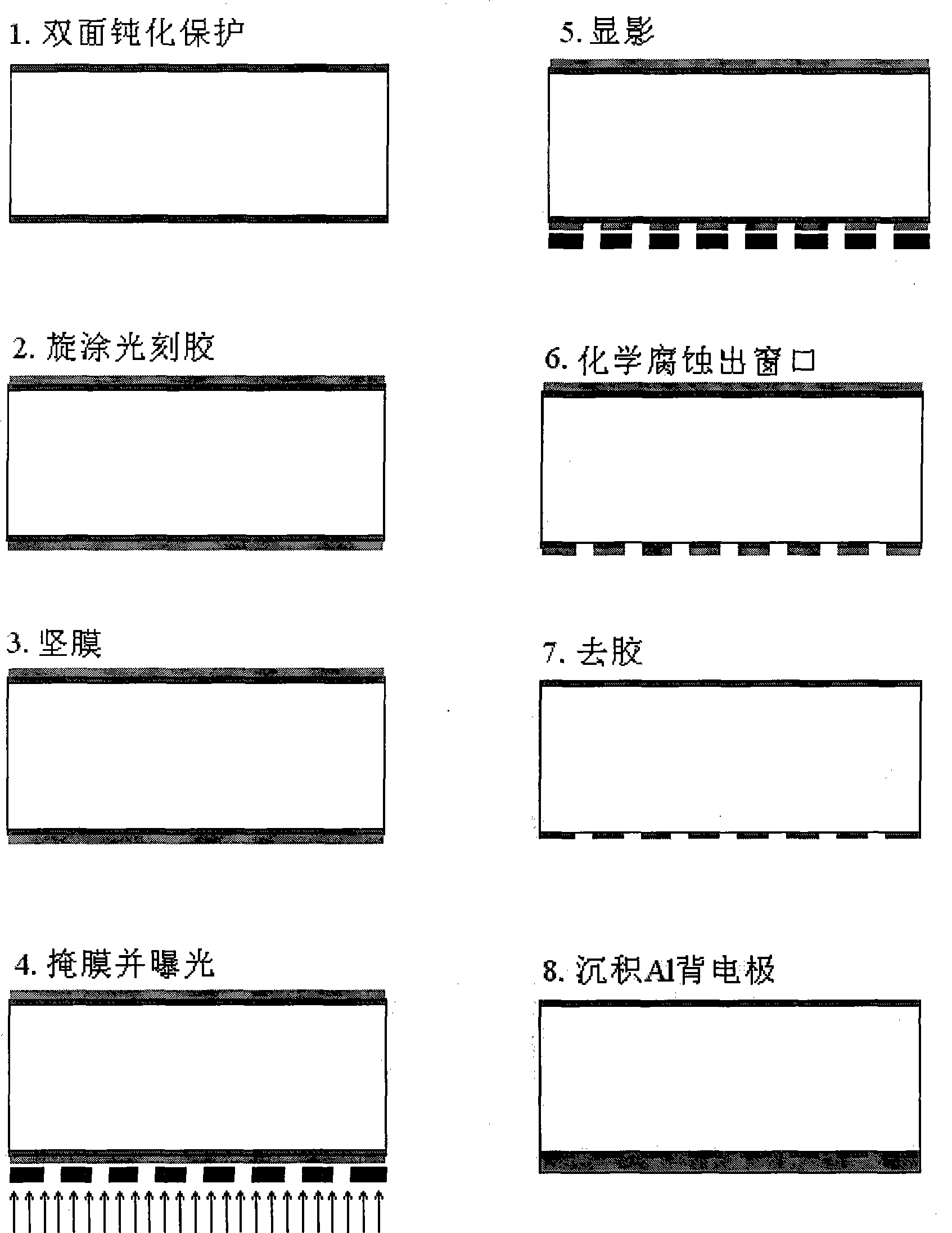
[0044] 4. Double-sided double-layer passivation. Use thermal oxidation, PECVD or PVD to form silicon nitride / silicon oxide film stacks on the front and rear surfaces of silicon wafers to further improve the effects of passivation, anti-reflection, and internal reflection.
[0045] 5. Laser dotting, forming a large number of electrode local contact windows at the passiv...
PUM
 Abstract
Description
Claims
Application Information