

Polishing composite for silicon wafer polishing
A technique for polishing compositions and silicon wafers, which is applied in the fields of polishing compositions containing abrasives, electrical components, semiconductor/solid-state devices, etc. It can solve the problems of low removal rate, many metal residues, and many surface defects, and achieve High-quality polishing, fast polishing rate, and less surface defects
- Summary
- Abstract
- Description
- Claims
- Application Information
AI Technical Summary
Problems solved by technology
Method used
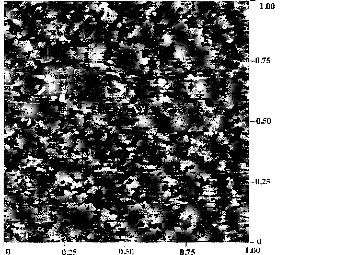
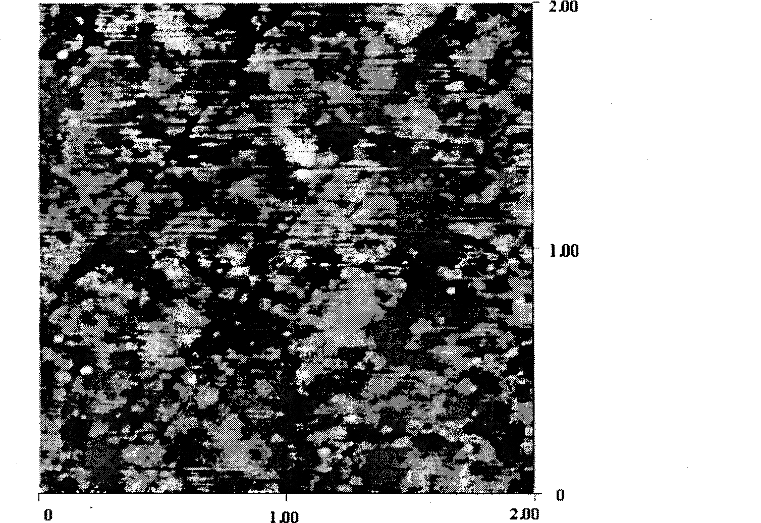
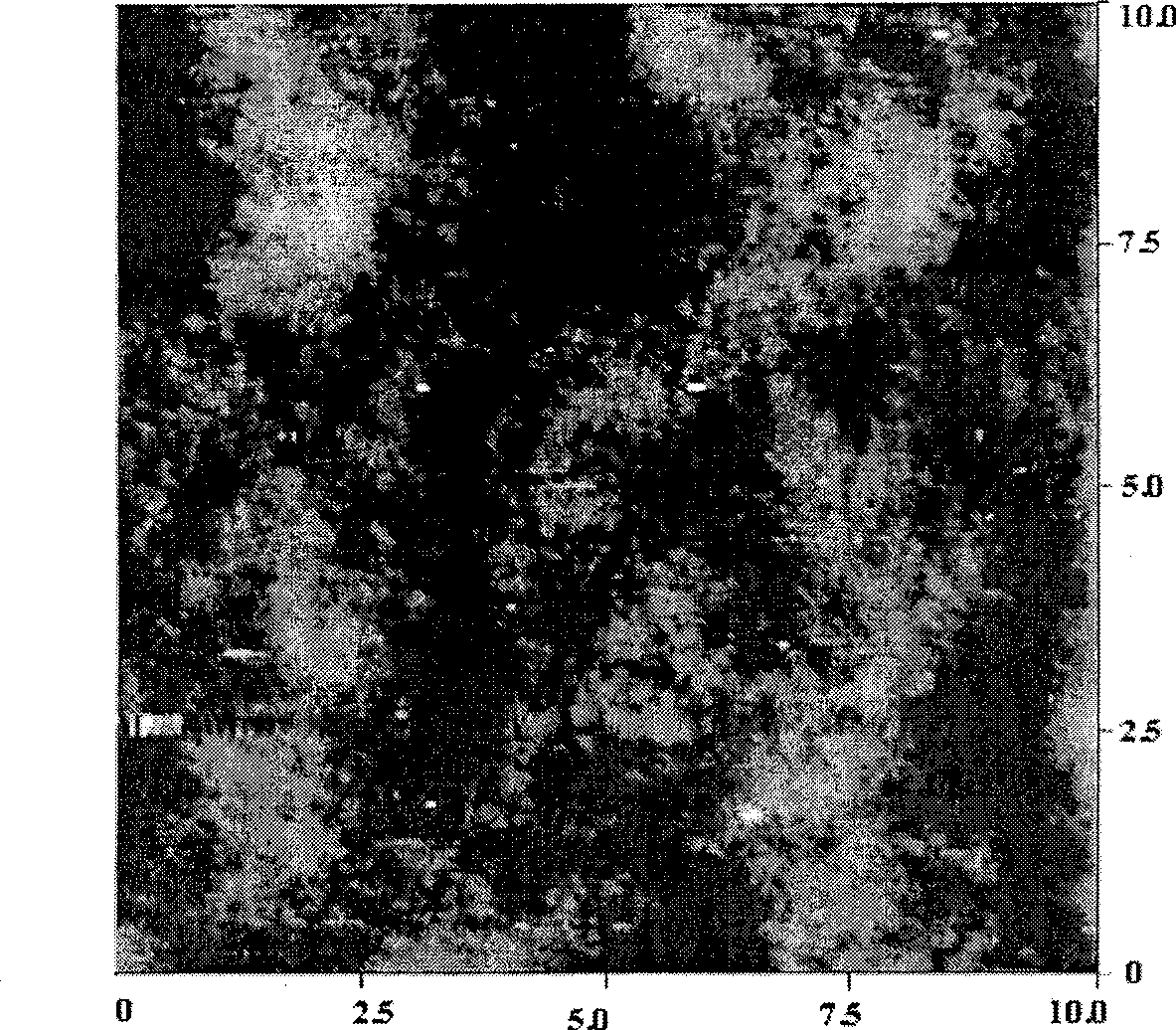
Image

Examples
Embodiment 1
[0047] Disperse 400g of colloidal silicon dioxide with a silicon dioxide content of 30% in 5464.4g of deionized water with a stirrer, add 120g of an aqueous solution containing 2% of dihydroxypropyl cellulose ether as a polishing interface control agent, and place in the stirrer Make the polishing interface control agent and colloidal silicon dioxide fully mixed; then add surfactant DC-193 (dimethylpolysiloxane polyether copolymer) 2.4g, chelating agent EDTA (ethylenediaminetetraacetic acid) 1.2g Add 12 g of basic compound TETA (triethylenetetramine), and finally filter the polishing composition with a filter element with a pore size of 0.5 μm, as shown in Table 1.
Embodiment 2~3
[0049] The preparation process was the same as in Example 1, and the amounts of the 2% aqueous solution of the polishing interface control agent dihydroxypropyl cellulose ether added were 180 g and 240 g, as shown in Table 1.
Embodiment 4
[0051] The preparation process is the same as in Example 1, dispersing 400 g of colloidal silicon dioxide with a silicon dioxide content of 30% in 5270.6 g of deionized water with a stirrer, and adding 2% dihydroxypropyl cellulose ether containing polishing interface control agent 300g of the aqueous solution, the polishing interface control agent and the colloidal silicon dioxide are fully mixed in the stirrer; then add the surfactant AEO-9 (polyoxyethylene (9) lauryl ether) 3.6g, the chelating agent TTHP (triethyl ether) successively Tetraamine hexaethylene phosphonic acid) 1.8g; Add two basic compounds DETA (triethylenetetramine) and PIZ (piperazine anhydrous), respectively 12g and 6g, and finally use a filter element with a pore size of 0.5 μm to The polishing compositions were filtered as shown in Table 1.
PUM
| Property | Measurement | Unit |
|---|---|---|
| Diameter | aaaaa | aaaaa |
| Resistivity | aaaaa | aaaaa |
Abstract
Description
Claims
Application Information