Wafer stage encapsulation LED chip and manufacturing method thereof

A light-emitting diode, wafer-level packaging technology, applied in semiconductor/solid-state device manufacturing, electrical components, electrical solid-state devices, etc., can solve the problems of poor heat dissipation, expensive equipment, and easy moisture.

Inactive Publication Date: 2009-06-10
杨秋忠
View PDF1 Cites 13 Cited by
  • Summary
  • Abstract
  • Description
  • Claims
  • Application Information

AI Technical Summary

Problems solved by technology

[0011] First of all, in the manufacturing process, it is necessary to increase the back-end packaging process, which will not only increase the process flow and time, but also need to add various equipment, such as wire bonding machines, flip chip machines, glue potting machines, molding machines or Testing equipment, etc., these equipments are extremely expensive, which greatly increases the manufacturing cost of light-emitting diode chips, and further affects the delivery deadline
[0012] Furthermore, the

Method used


Image

  • Wafer stage encapsulation LED chip and manufacturing method thereof
  • Wafer stage encapsulation LED chip and manufacturing method thereof
  • Wafer stage encapsulation LED chip and manufacturing method thereof

Examples


Embodiment Construction

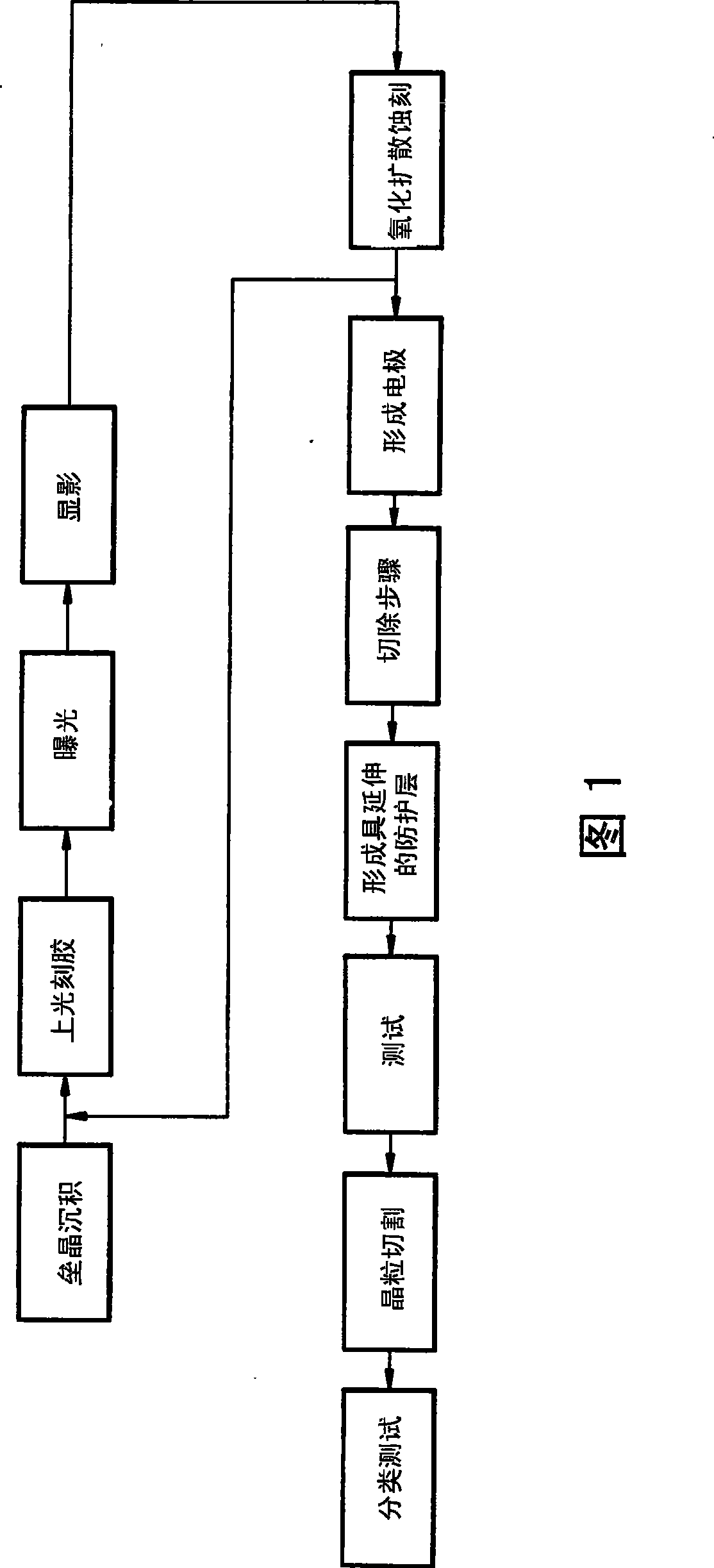
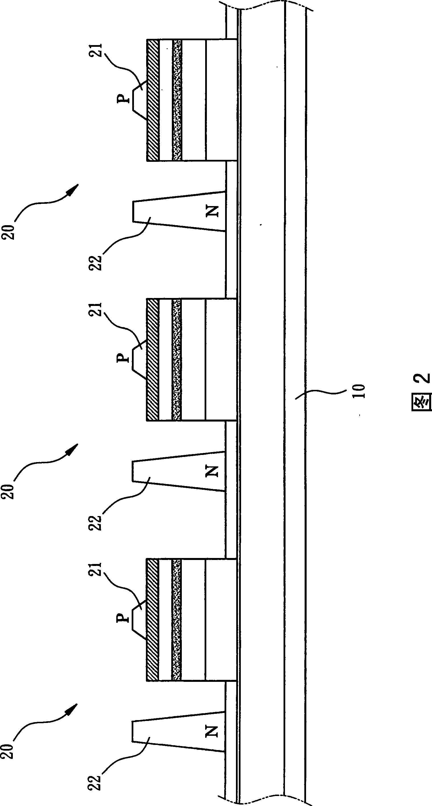
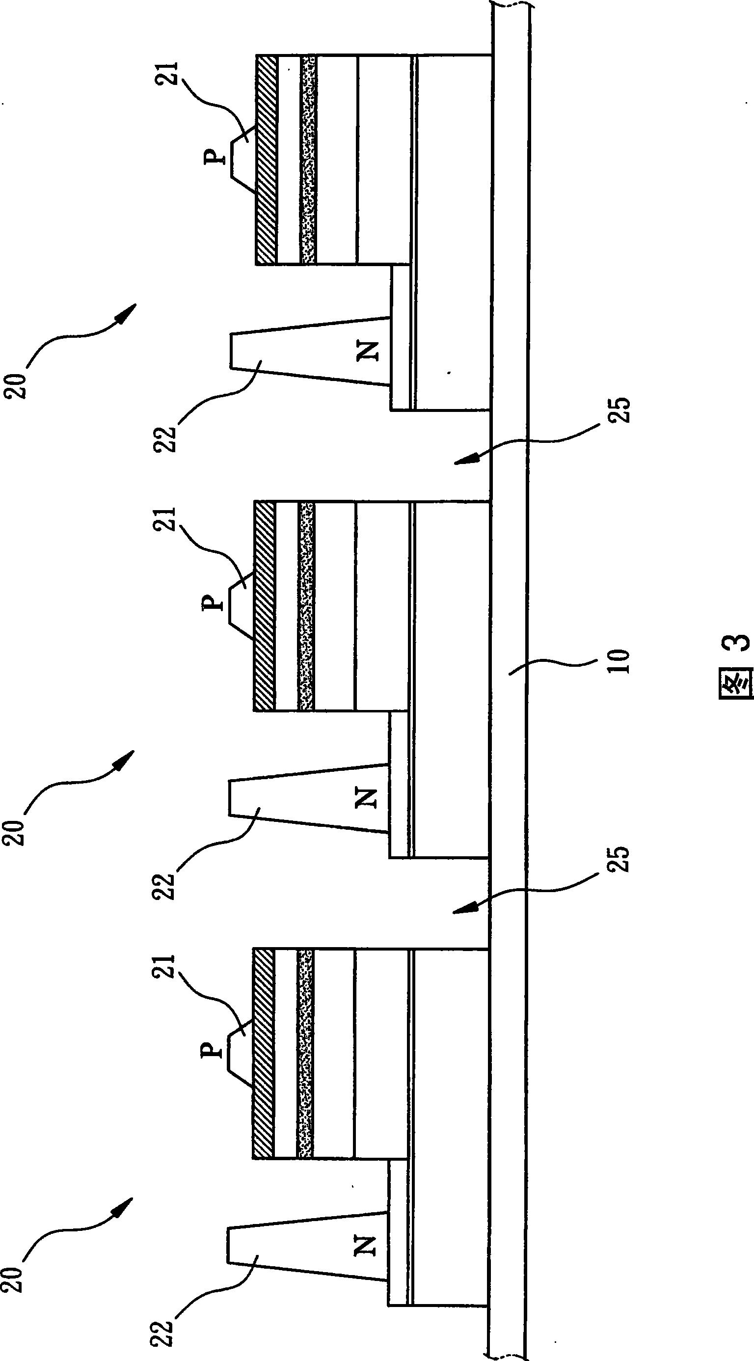
[0037] The present invention is a wafer-level packaged light-emitting diode chip and a manufacturing method thereof. As shown in FIGS. 1, 2, 5 and 8, the light-emitting diode chip (Light Emitting Diodes, LED) is mounted on a wafer substrate (Wafer) utilizes steps such as photoresist, exposure, development and oxidation diffusion etching of the semiconductor process to form light-emitting diodes 20 (as shown in FIG. 2 ) with many connections. Each light-emitting diode 20 has a positive surface electrode 21 (P pole electrode) and a negative electrode 22 (N pole electrode), and utilize a cutting step to remove the epitaxial layer connected to the adjacent light emitting diode 20 to form a cutout region 25 ( As shown in FIG. 3 ), and utilize a step of forming an extended protective layer to form a protective layer 30 (as shown in FIG. shown), the protective layer 30 is an insulating material with high light transmittance or high reflectivity and has protective functions such as mo...


PUM


Abstract

The invention provides a wafer-level packaged LED chip, and a manufacture method thereof. The method is characterized in that an LED is formed on a wafer substrate by utilizing the steps of smearing photoresist, exposing, developing, etching and the like in a semiconductor process; the top surface of the LED is provided with a positive electrode and a negative electrode; before the wafer substrate is cut into a single LED chip, an extension layer connected with the adjacent LED is removed through a cutoff step; through a step of forming protective layers with extensions, a protective layer with an extension is formed on the periphery of the LED except the top surfaces of the positive and negative electrodes, so as to ensure that the LED chip can utilize the protective layer to generate self-protection functions of resisting moisture, preventing oxidation, preventing short circuit and the like; therefore, subsequent assembly routing, packaging, package test and other actions can be reduced; and the method can greatly shorten production flow and time, reduce production cost, raise product yield, and then increases economic benefit.

Description

technical field [0001] The present invention belongs to a self-protection technology of a light-emitting diode chip, and specifically refers to a light-emitting diode chip (chip) packaged at the wafer level with self-protection functions such as moisture resistance, oxidation resistance, and short circuit prevention, and a manufacturing method thereof . Background technique [0002] Press, the making of existing light-emitting diode chip (Light EmittingDiodes, LED) is shown in Figure 10, after completing the wafer substrate (substrate) making of smelting, crystal pulling, crystal column slicing and wafer polishing, on the wafer (Wafer ) on the substrate 50, a plurality of connected light-emitting diodes 60 (as shown in FIG. surface and has a positive electrode 61 (P pole electrode) and a negative electrode 62 (N pole electrode), and forms a The protective layer 70 (as shown in FIG. 12 ), and then utilize cutting techniques such as laser cutting (laser cutting), water jet, ...

Claims


Application Information

Patent Timeline
IPC IPC(8): H01L33/00H01L21/50H01L21/56H01L21/78H01L23/29H01L23/31
Inventor 杨秋忠
Owner 杨秋忠
Why Eureka
Try Eureka