

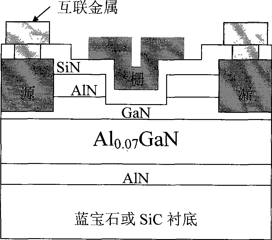
AlN/GaN enhancement type metal-insulator-semiconductor field effect transistor and method of producing the same
A field effect transistor and manufacturing method technology, applied in the field of microelectronics, can solve the problems of large channel transmission resistance, small output current, large noise, etc., and achieve the effects of large threshold voltage, large output current, and high output current
- Summary
- Abstract
- Description
- Claims
- Application Information
AI Technical Summary
Problems solved by technology
Method used
Image

Examples
Embodiment 1
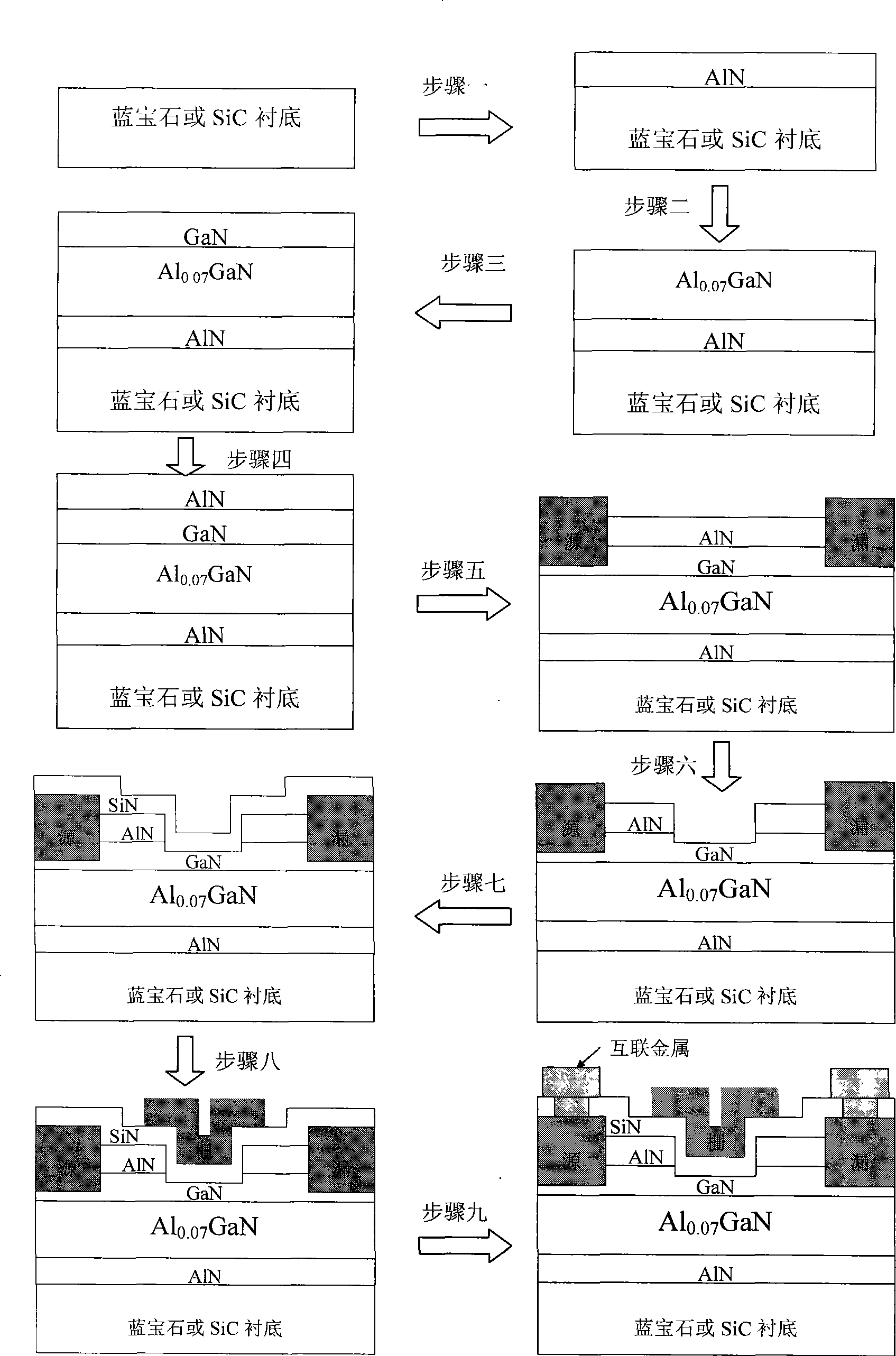
[0052] Embodiment 1, fabricating an AlN / GaN enhanced metal-insulator-semiconductor field-effect transistor with an AlN barrier layer of 3nm thickness on a sapphire substrate, the steps are as follows:
[0053] In step 1, an AlN nucleation layer is grown on the sapphire substrate by MOCVD process.
[0054] (1a) Put the sapphire substrate into the reaction chamber of the metal-organic chemical vapor deposition MOCVD equipment, when the vacuum degree of the reaction chamber drops to 1×10 -2 After Torr, the sapphire substrate is subjected to high-temperature heat treatment and surface nitriding under the protection of a mixed gas of hydrogen and ammonia. The heating temperature is 1050°C, the heating time is 5min, and the reaction pressure is kept at 40Torr. The ammonia gas flow rate is 1500 sccm, and the hydrogen gas flow rate is 1500 sccm;
[0055] (1b) Lower the substrate temperature to 500° C., and grow an AlN nucleation layer with a thickness of 30 nm. The reaction pressure...
Embodiment 2
[0080] Embodiment 2, fabricating an AlN / GaN enhanced metal-insulator-semiconductor field effect transistor with an AlN barrier layer of 3.6nm thickness on a SiC substrate, the steps are as follows:
[0081] In step 1, an AlN nucleation layer is grown on the SiC substrate by using an MOCVD process.
[0082] (1a) Put the SiC substrate into the reaction chamber of the metal organic chemical vapor deposition MOCVD equipment, when the vacuum degree of the reaction chamber drops to 1×10 -2 After Torr, the sapphire substrate is subjected to high-temperature heat treatment and surface nitriding under the protection of a mixed gas of hydrogen and ammonia. The heating temperature is 1050°C, the heating time is 5min, and the reaction pressure is kept at 40Torr. The ammonia gas flow rate is 1500 sccm, and the hydrogen gas flow rate is 1500 sccm;
[0083] (1b) Lower the substrate temperature to 900° C., and grow an AlN nucleation layer with a thickness of 30 nm. The reaction pressure was...
Embodiment 3
[0108] Embodiment 3, making an AlN / GaN enhanced metal-insulator-semiconductor field-effect transistor with an AlN barrier layer of 3.3 nm thick on a sapphire substrate, the steps are as follows:
[0109] In step 1, an AlN nucleation layer is grown on the sapphire substrate by MOCVD process.
[0110] (1a) Put the sapphire substrate into the reaction chamber of the metal-organic chemical vapor deposition MOCVD equipment, when the vacuum degree of the reaction chamber drops to 1×10 -2 After Torr, the sapphire substrate is subjected to high-temperature heat treatment and surface nitriding under the protection of a mixed gas of hydrogen and ammonia. The heating temperature is 1050°C, the heating time is 5min, and the reaction pressure is kept at 40Torr. The ammonia gas flow rate is 1500 sccm, and the hydrogen gas flow rate is 1500 sccm;
[0111] (1b) Lower the substrate temperature to 500° C., and grow an AlN nucleation layer with a thickness of 30 nm. The reaction pressure was k...
PUM
| Property | Measurement | Unit |
|---|---|---|
| Thickness | aaaaa | aaaaa |
Abstract
Description
Claims
Application Information