Preparation of boron doped diamond superconduction material

A technology of superconducting materials and diamond, which is applied in metal material coating process, gaseous chemical plating, coating, etc., can solve the problem that the superconducting transition temperature of diamond film is not high enough, the film forming area is difficult to expand, and the effective doping concentration is not high enough. Advanced problems, to achieve the effect of inhibiting the loss of active boron atoms, simple structure, and improving production efficiency

Inactive Publication Date: 2009-07-15
INST OF PHYSICS - CHINESE ACAD OF SCI
View PDF0 Cites 16 Cited by
  • Summary
  • Abstract
  • Description
  • Claims
  • Application Information

AI Technical Summary

Problems solved by technology

[0003] The object of the present invention is: in order to solve the existing process of using high temperature and high pressure sintering technology to prepare boron-doped diamond superconducting particles, the boron-doped superconducting diamond is obtained by mutual diffusion and reaction of two substances, wherein The boron content is not only difficult to control, but also unevenly distributed, as well as the problems of low effective doping concentration

Method used


Image

  • Preparation of boron doped diamond superconduction material
  • Preparation of boron doped diamond superconduction material
  • Preparation of boron doped diamond superconduction material

Examples


Embodiment 1

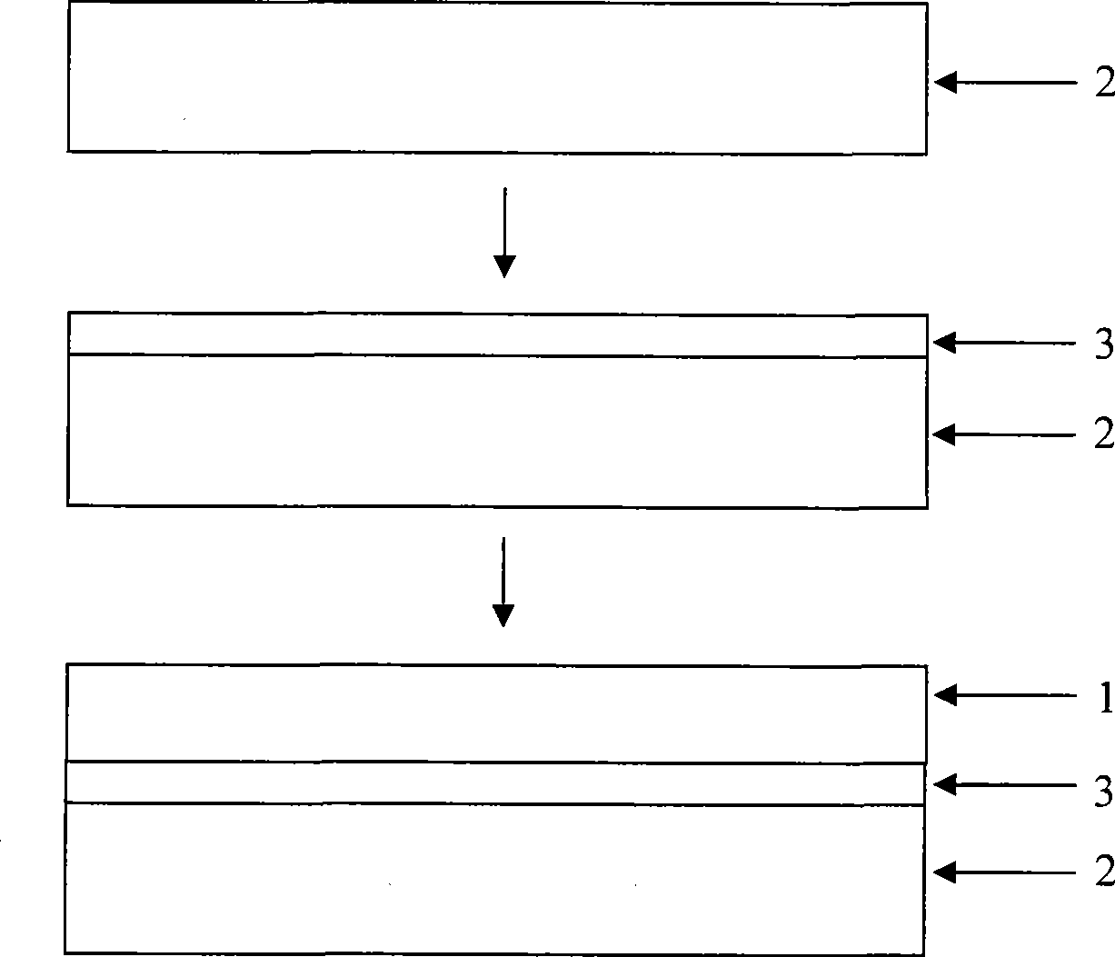
[0034] refer to image 3 , carried out in a hot filament chemical vapor deposition system, the method of the present invention is described in detail through the following specific steps.

[0035] 1. First, pretreat the inner wall of the cavity of the hot filament chemical vapor deposition system by hot filament chemical vapor deposition of boron-doped diamond film. Pretreatment conditions: the flow rates of methane and hydrogen are 8 sccm and 100 sccm respectively At the same time, the hydrogen gas with a flow rate of 10 sccm is introduced, and the hydrogen gas enters the cavity of the deposition system after passing through the container containing trimethyl borate—hereinafter referred to as "hydrogen gas carrying trimethyl borate", that is, the flow rate of hydrogen gas carrying trimethyl borate is 10sccm, the reaction pressure in the cavity is 25 Torr, the filament temperature is about 2200°C, and the pretreatment is carried out for 10 hours; under the above conditions, th...

Embodiment 2

[0042] refer to image 3 , the method of the present invention is described in detail through the following specific steps.

[0043] 1. First, the inner wall of the cavity of the hot filament chemical vapor deposition system is pretreated by the method of hot filament chemical vapor deposition of a boron-doped diamond film, and the remaining pretreatment conditions and pretreatment time are completely the same as in Example 1;

[0044] 2. With a polished N-type (001) single crystal silicon wafer as the substrate, take an alcohol solution in which diamond powder with a particle size of 0.2 microns is dissolved, put the single crystal silicon into the solution and perform ultrasonication for 60 minutes, and the silicon substrate Diamond nucleation points are generated on the bottom, and then the cleaning process for semiconductor material preparation is carried out, such as cleaning with cleaning solutions such as acetone, ethanol or deionized water;

[0045] 3. Deposit diamond...

Embodiment 3

[0049] refer to image 3 , the method of the present invention is described in detail through the following specific steps.

[0050] 1. First, pretreat the inner wall of the cavity of the hot filament chemical vapor deposition system by hot filament chemical vapor deposition of boron-doped diamond film. Pretreatment conditions: the flow rates of methane and hydrogen are 8 sccm and 100 sccm respectively At the same time, the flow rate of hydrogen carrying trimethyl borate is 6 sccm, the reaction pressure in the chamber is 40 Torr, the temperature of the filament is about 2200 ° C, and the pretreatment is carried out for 25 hours;

[0051] 2. With a polished N-type (001) single crystal silicon wafer as the substrate, take an alcohol solution in which diamond powder with a particle size of 0.2 microns is dissolved, put the single crystal silicon into the solution and perform ultrasonication for 60 minutes, and the silicon substrate Diamond nucleation points are produced on the b...


PUM

PropertyMeasurementUnit
Thicknessaaaaaaaaaa
Carrier concentrationaaaaaaaaaa

Abstract

The invention relates to a preparation method of boron dope diamond superconducting material, including the following steps: traditional synthetic boron dope diamond technology is used for carrying out pretreatment on an internal cavity body, a clean substrate is placed on the substrate pad of the inner cavity after pretreatment, and the traditional hot-filament chemical vapor deposition method is used for depositing a diamond film transition layer; the deposit growth conditions are as follows: the voltage bias applied on the substrate is zero, reaction gases of methane and hydrogen are led in through two paths, the volume ratio of the two paths of gases is (2-10): 100, the temperature of the substrate is in the range from 800 DEG to 1000 DEG by adjusting the distance between the substrate and the filament, the gas pressure is 20-60 Torr, and the growth time lasts 0.5-1.5 hours; the growth conditions of compositing the diamond film transition layer are remained, and the boron dope diamond superconducting material is continuously grown for at least 3 hours to obtain the boron dope diamond superconducting material. The method not only has the advantages of low cost and high flexibility but also obtains the boron dope diamond superconducting material with higher carrier concentration and higher superconducting transition temperature.

Description

technical field [0001] The invention relates to a preparation method of a boron-doped diamond superconducting material, in particular to a process of combining the cavity inner wall pretreatment technology with pre-deposition of a diamond film transition layer on a substrate by using a hot filament chemical vapor deposition system. A method for preparing a boron-doped diamond superconducting material on a non-diamond substrate. Background technique [0002] The synthesis and characterization of doped diamond materials have always been the focus of attention, especially the synthesis of boron-doped diamond superconducting materials and the characterization of their superconducting properties have been research hotspots in the past two years, among which boron-doped diamond materials The design and preparation of nanomaterials are the basis and key to achieve the purpose of superconductivity. There are mainly two methods for preparing boron-doped diamond superconducting mater...

Claims


Application Information

Patent Timeline
IPC IPC(8): C23C16/22
Inventor 顾长志王宗利路超罗强李俊杰金爱子杨海方
Owner INST OF PHYSICS - CHINESE ACAD OF SCI
Why Eureka
Try Eureka