

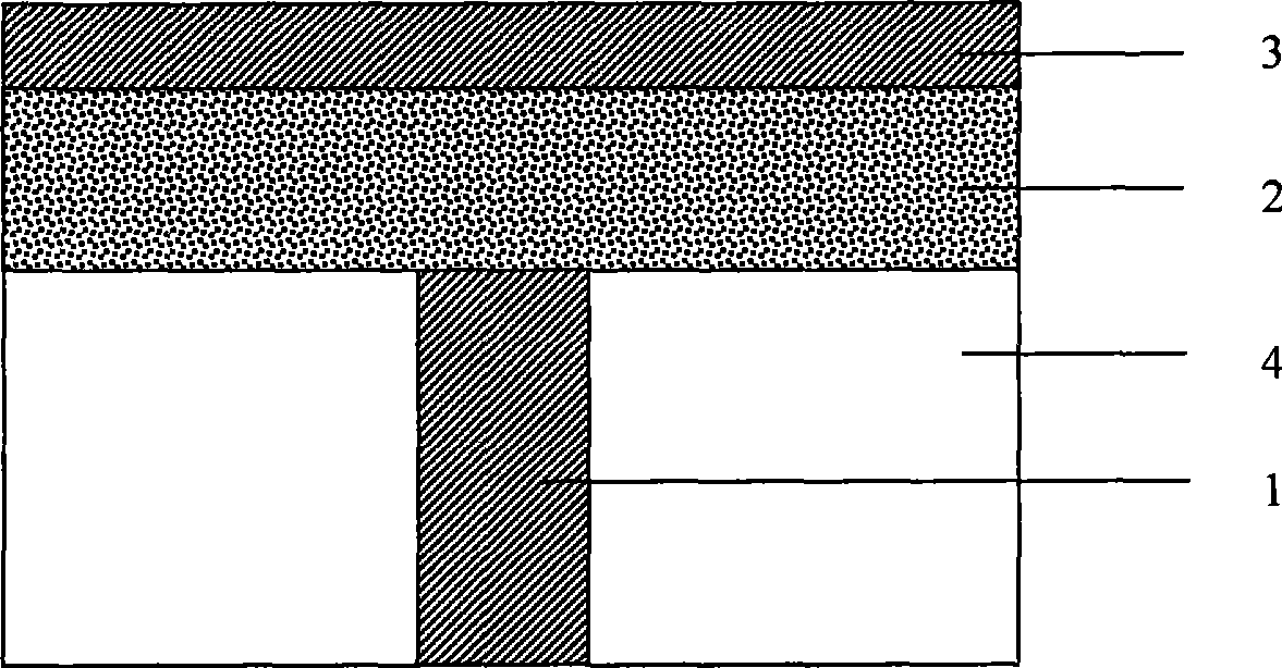
M-Sb-Se phase changing thin-film material used for phase changing memory
A phase change memory and thin film material technology, applied in the field of microelectronics, can solve the problems of phase change memory application limitations, poor CMOS process compatibility, poor thermal stability, etc., and achieve good data retention characteristics, good compatibility, and fast crystallization speed. Effect
- Summary
- Abstract
- Description
- Claims
- Application Information
AI Technical Summary
Problems solved by technology
Method used
Image

Examples
Embodiment 1
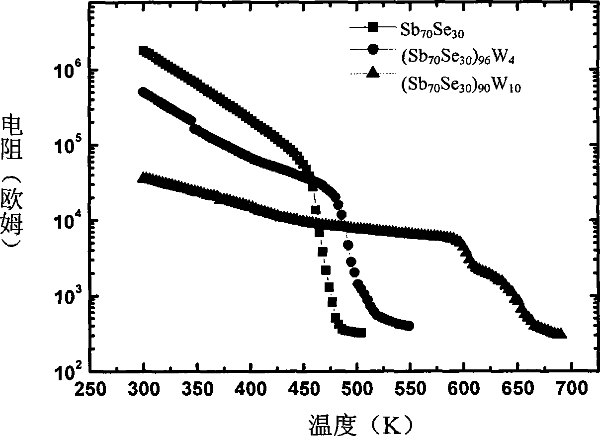
[0027] In this embodiment, tungsten (W) element is used as M doping element, the content x of Sb is 65%-80 atomic percent, and the content y of W is 2%-6 atomic percent.
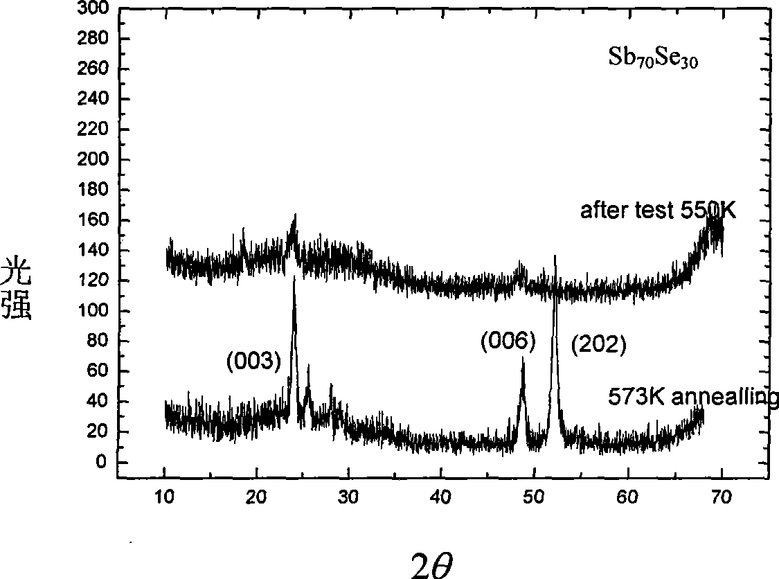
[0028] When the film is in an amorphous state, the film resistance is in a high-resistance state. As the temperature increases, the film begins to crystallize and undergo a phase transition, and at the same time shows a decrease in resistance. After the film crystallizes, the film resistance is in a low-resistance state. Phase-change memory devices can be realized by applying electric pulses, and amorphous high resistance and polycrystalline low resistance can be reversibly switched by applying pulses. Such as figure 2 As shown, in the relationship between resistance and annealing temperature of W-Sb-Se thin film with tungsten (W) content, the crystallization temperature of W-Sb-Se thin film increases with the increase of w content. When the composition of the phase change film material is (Sb 70 Se 30 )...
Embodiment 2
[0035] In this embodiment, aluminum (Al) is used as M doping element, the content x of Sb is 65%-80 atomic percent, and the content y of Al is 2%-10 atomic percent.
[0036] see Figure 5 , when the film is in an amorphous state, the film resistance is in a high-resistance state. As the temperature increases, the film begins to crystallize and undergo a phase transition, and at the same time shows a decrease in resistance. When the film crystallizes, the film resistance is in a low-resistance state. This process In phase-change memory devices, it can be realized by applying electric pulses, and amorphous high resistance and polycrystalline low resistance can be reversibly switched by applying pulses. In the relationship curve between the resistance of the Al-Sb-Se thin film and the annealing temperature, the crystallization temperature of the Al-Sb-Se thin film increases with the increase of the Al content. When the composition of the phase change film material is (Sb 70 Se ...
PUM
| Property | Measurement | Unit |
|---|---|---|
| Crystallization temperature | aaaaa | aaaaa |
| Melting point | aaaaa | aaaaa |
| Crystallization temperature | aaaaa | aaaaa |
Abstract
Description
Claims
Application Information