Surface plasmon crystal transducer and preparation method thereof
A surface plasmon and sensor technology, applied in the field of plasmon crystal sensor and its preparation, can solve the problem of low sensitivity, achieve high sensitivity, good comprehensive index, and reduce the effect
- Summary
- Abstract
- Description
- Claims
- Application Information
AI Technical Summary
Problems solved by technology
Method used
Image
Examples
Embodiment 1
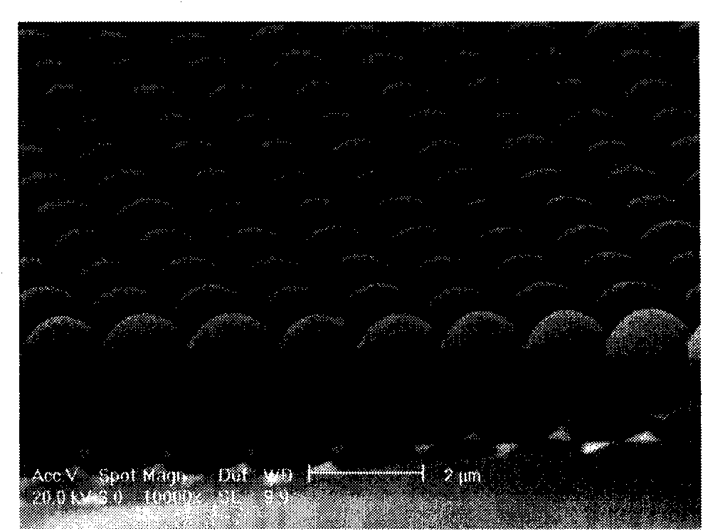
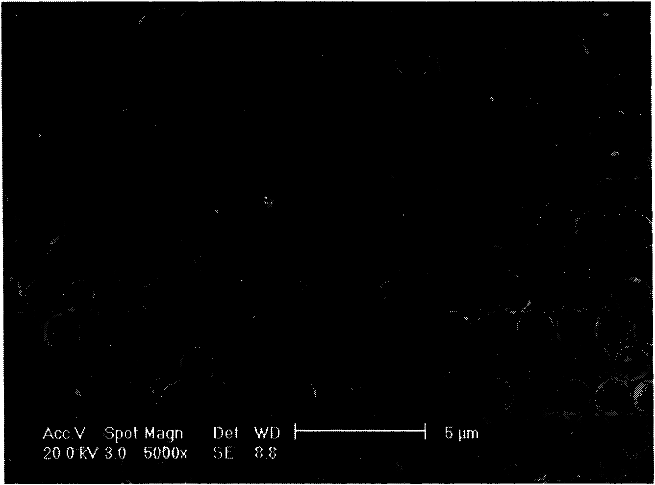
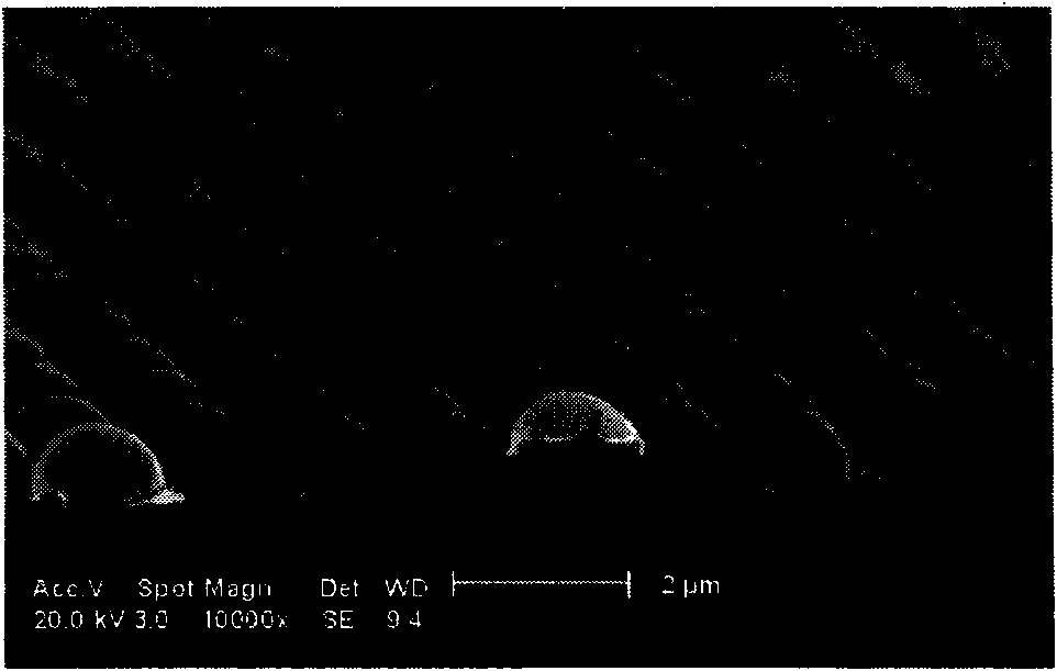
[0028] Embodiment 1: In this example, monodisperse silica microspheres with a diameter of 1580 nanometers were selected. First, two-dimensional hexagonal close-packed colloidal crystals are assembled on a quartz substrate (see authorized patents ZL 03 1 31989.0 and ZL 2004 1 0041939.9). Secondly, the argon ion sputtering coating method is used to directly deposit a layer of gold film on the surface of the microsphere template, and the deposition time is controlled so that the thickness of the apex of the gold hemispherical shell is about 50 nanometers (see patent application 200610039478.0). The silicon dioxide sacrificial template was then removed by hydrofluoric acid vapor etching to obtain a surface plasmon crystal sensor composed of interconnected gold nano-hollow hemispherical shells. Finally, the surface plasmon sensor located on the flat quartz substrate is immersed in the solution to be measured to measure the optical transmission spectrum.
Embodiment 2
[0029] Embodiment 2: In this example, monodisperse silica microspheres with a diameter of 1000 nanometers were selected. First, two-dimensional hexagonal close-packed colloidal crystals are self-assembled on a glass substrate. Secondly, the argon ion sputtering coating method is used to directly deposit a layer of platinum film on the surface of the microsphere template, and the deposition time is controlled so that the thickness of the apex of the platinum hemispherical shell is about 100 nanometers. The silicon dioxide sacrificial template was then removed by hydrofluoric acid vapor etching to obtain a surface plasmon crystal sensor composed of interconnected platinum nano-hollow hemispherical shells. Finally, the surface plasmon crystal sensor located on the flat glass substrate is immersed in the solution to be measured to measure the optical transmission spectrum.
Embodiment 3
[0030] Embodiment 3: In this example, monodisperse silica microspheres with a diameter of 490 nanometers were selected. First, two-dimensional hexagonal close-packed colloidal crystals are self-assembled on a glass substrate. Secondly, a magnetron sputtering method is used to directly deposit a layer of aluminum film on the surface of the microsphere template, and the deposition time is controlled so that the thickness of the apex of the aluminum hemispherical shell is about 50 nanometers. Then, the silicon dioxide sacrificial template was removed by vapor etching of hydrofluoric acid, and a surface plasmon crystal sensor composed of interconnected aluminum nano-hollow hemispherical shells was obtained. Finally, the surface plasmon crystal sensor located on the flat glass substrate is immersed in the solution to be measured to measure the optical transmission spectrum.
PUM
| Property | Measurement | Unit |
|---|---|---|
| Thickness | aaaaa | aaaaa |
| Diameter | aaaaa | aaaaa |
| Diameter | aaaaa | aaaaa |
Abstract
Description
Claims
Application Information


