Method for producing leadless brazing alloy salient point by laser

A lead-free solder and laser technology, applied in laser welding equipment, manufacturing tools, semiconductor/solid-state device manufacturing, etc., can solve the problem of oversized solder bump size device packaging, slow solder bump production speed, and automation No problems such as high level, to achieve the effect of reducing processing cost, fast processing speed and small size

Inactive Publication Date: 2009-10-14
SOUTH CHINA UNIV OF TECH
View PDF0 Cites 14 Cited by
  • Summary
  • Abstract
  • Description
  • Claims
  • Application Information

AI Technical Summary

Problems solved by technology

However, the existing laser methods for making solder bumps either use solder containing harmful substances such as lead, which can damage or destroy the human brain center, peripheral nervous system, hematopoietic system, reproductive system, and even the heart. Function; either shielding gas will be used, which will complicate the processing technology and increase the production cost to a certain extent
At the same time, the existing laser method for making solder bumps requires inert gas protection and a preheating process in the manufacturing process, as well as the large spot size of the laser equipment used, making the solder bumps faster. Slow, the size of solder bumps is too large to meet the needs of small device packaging, and its degree of automation is not high

Method used


Image

  • Method for producing leadless brazing alloy salient point by laser
  • Method for producing leadless brazing alloy salient point by laser

Examples


Embodiment

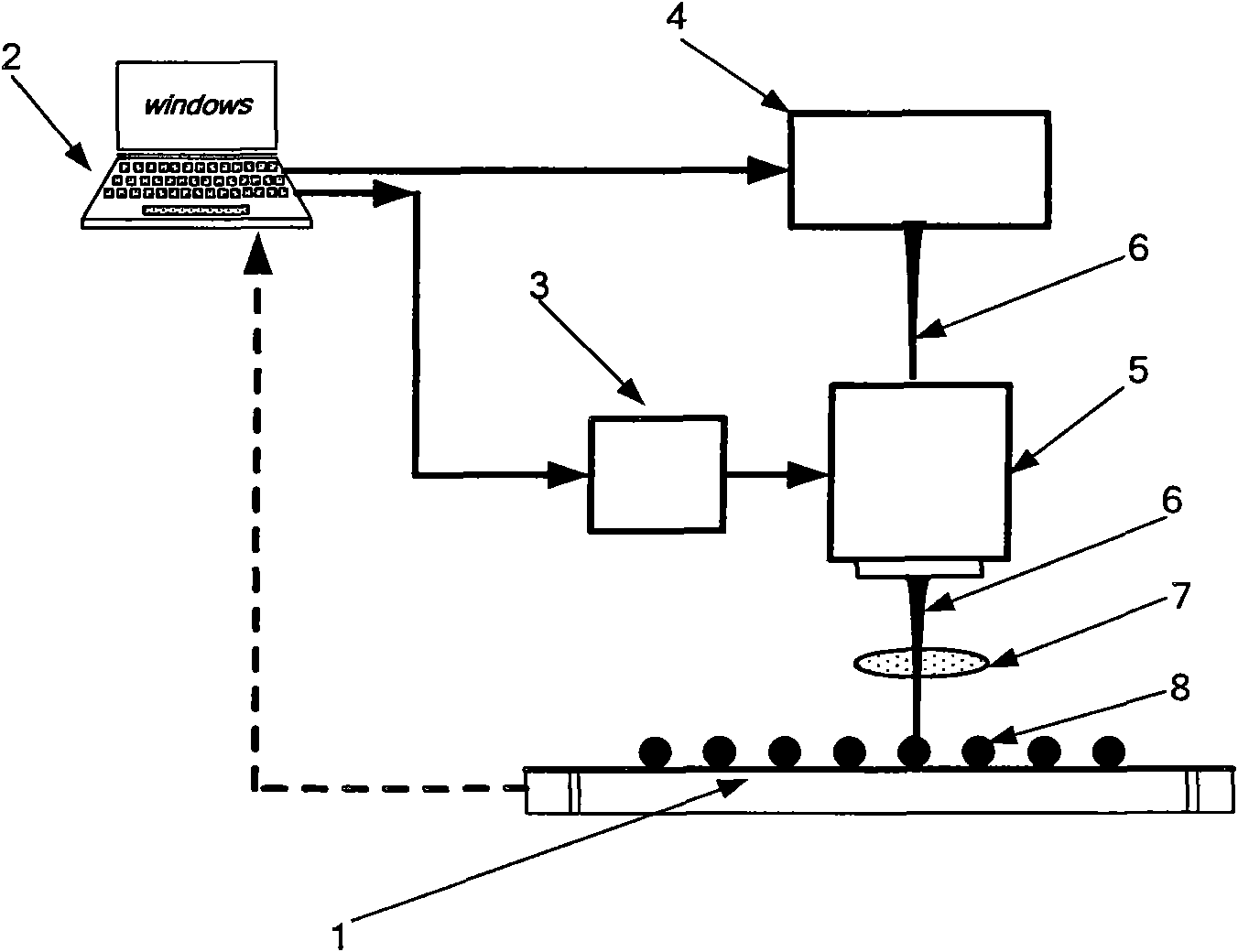
[0034] In this embodiment, a method of laser making lead-free solder bumps, such as figure 1 As shown in the schematic diagram of the system structure, it specifically includes the following steps:

[0035] (1) Apply lead-free solder on the position where the substrate 1 is used for ball planting (i.e., the making of solder bumps), and place the substrate 1 coated with lead-free solder on the processing plane of the laser manufacturing system (i.e. On the focal plane of the f-θ flat-field lens 7 in the laser production system);

[0036] (2) Input the position data of the ball planting place of the substrate 1 into the computer 2, and the programmed program (ie path planning program) in the computer 2 will update the data, and plan the ball planting path according to the position data of the ball planting place ;

[0037] (3) The computer 2 forms a control signal with the planned ball planting path, and sends it to the control unit 3 and the laser 4 respectively through the U...


PUM

PropertyMeasurementUnit
diameteraaaaaaaaaa

Abstract

The invention provides a method for producing a leadless brazing alloy salient point by laser, comprising: coating leadless brazing alloy on the position for planting a ball on a substrate and placing the substrate on a process plane; then inputting the position data of the substrate ball planting position into a computer followed by computer programming for ball planting route planning; forming control signals of the planned ball planting route and sending the formed control signals into a control member and a laser by the computer; sequentially setting the various processing parameters; controlling a scanning galvanometer to work in cooperation with the laser by the control member, scanning the substrate coated with the leadless brazing alloy according to the ball planting route by the laser beam followed by the melting of the leadless brazing alloy; then moving the laser beam away, solidifying the leadless brazing alloy, forming metallurgical bonding with the substrate, and so far forming the leadless brazing alloy salient point. The leadless brazing alloy salient point produced by the invention is environment-friendly, harmless to human body, and the invention has fast processing and high processing accuracy, the processing requires no protection gas, so that the processing is simple and the automation degree is high.

Description

technical field [0001] The invention relates to the technical field of microelectronic packaging, in particular to a method for manufacturing lead-free solder bumps by laser. Background technique [0002] In the field of microelectronic packaging, the production of solder bumps is one of the key technologies in packaging such as BGA (Ball Grid Array) and CSP (Chip Scale Package). There are many ways to make solder bumps. Among them, the laser method to produce solder bumps overcomes many shortcomings of traditional production methods, and thus has been widely recognized by peer experts. [0003] In recent years, with the development of laser technology, laser solder bump technology has also developed rapidly. Wang Qingchun and others from Harbin Institute of Technology in China have carried out in-depth and detailed research on this technology, and have achieved certain results; conducted research and obtained satisfactory results; Zou Xinjue and others from Shanghai Jiao...

Claims


Application Information

Patent Timeline
Patent Type & Authority Applications(China)
IPC IPC(8): H01L21/60B23K26/20B23K26/34
Inventor 师文庆杨永强
Owner SOUTH CHINA UNIV OF TECH
Why Eureka
Try Eureka