Semiconductor film of organic film solar battery as well as forming method and manufacturing method thereof

A technology for solar cells and organic thin films, which is applied in the manufacture of semiconductor/solid-state devices, semiconductor devices, and electric solid-state devices, etc., can solve the problems of reduced service life, unstable morphology, and inability to effectively control the morphology, and can improve the current , the effect of increasing the junction area

Inactive Publication Date: 2009-11-18
RYTEC CORP
View PDF0 Cites 0 Cited by
  • Summary
  • Abstract
  • Description
  • Claims
  • Application Information

AI Technical Summary

Problems solved by technology

However, the morphology of this heterojunction structure is unstable, and it is prone to phase separation under certain conditions such as light and high temperature, which greatly reduces the service life of the device.
[0008] In addition, the morphology of the heterojunction structure is highly related to the solvent used during coating, and in the process of forming the h

Method used


Image

  • Semiconductor film of organic film solar battery as well as forming method and manufacturing method thereof
  • Semiconductor film of organic film solar battery as well as forming method and manufacturing method thereof
  • Semiconductor film of organic film solar battery as well as forming method and manufacturing method thereof

Examples


Example Embodiment

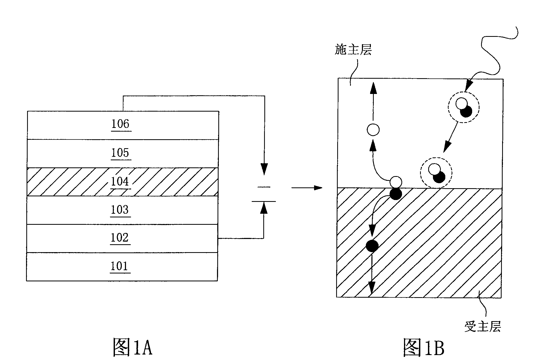
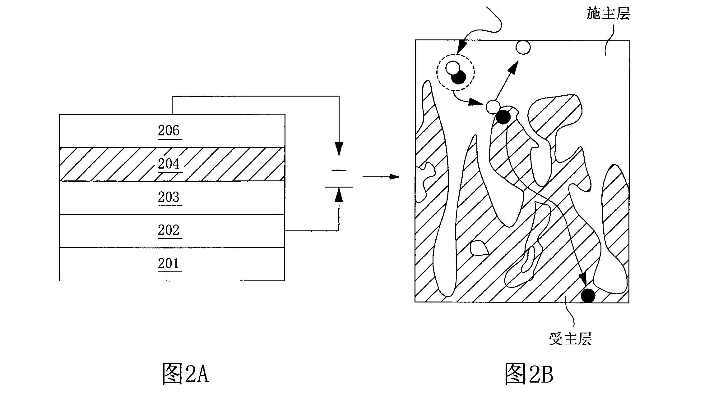
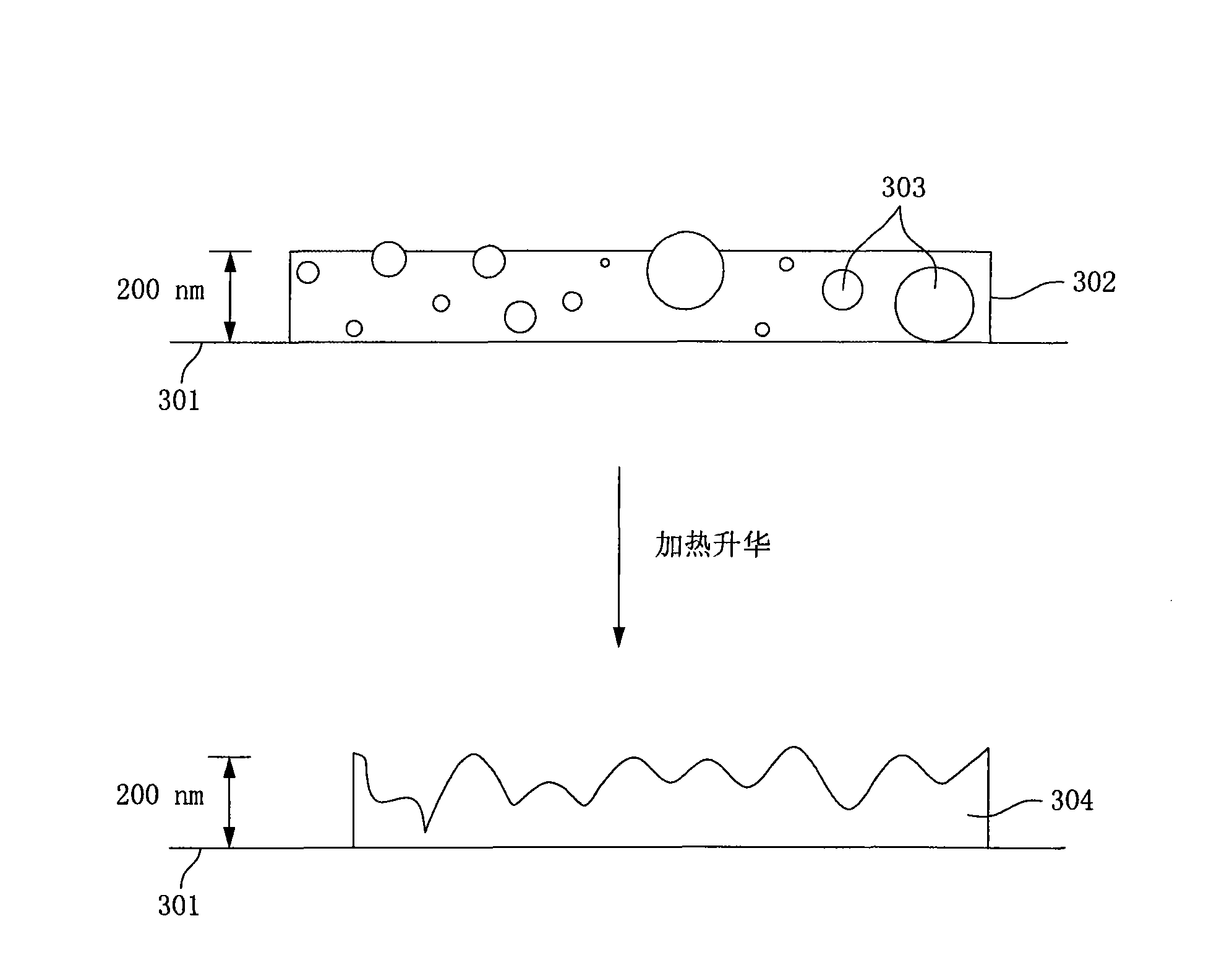
[0045] Generally speaking, the present invention is achieved by adding a solid substance to a coating liquid of a semiconductor material; coating the coating liquid on an interface; and removing the solid by sublimation during the formation of the semiconductor thin film. Type material to obtain a semiconductor film with a rough surface.

[0046]Up to now, there are two main methods for making microporous in polymer film to control the roughening of the surface. One is to use the principle of phase separation of two incompatible polymers, which is decomposed by heating after phase separation. , Radiation decomposition or hydrolysis method to crack and remove one of the polymers to form a thin film with microporosity. The other method is to use block copolymers to form different morphology, plus heating Decomposition, radiation decomposition, or hydrolysis is used to crack and remove one of the polymers to form a thin film with micropores. The above methods all involve molecular ch...


PUM


Abstract

The invention relates to an organic film solar battery element as well as a forming method and a manufacturing method thereof. The organic film solar battery element at least comprises a semiconductor film layer with a rough surface. The semiconductor film layer with the rough surface can be a P type semiconductor layer or an N type semiconductor layer, and a rough appearance is generated on a joint surface of the P type semiconductor layer and the N type semiconductor layer.

Description

technical field [0001] The present invention relates to an organic thin film solar cell, and in particular to a donor layer or acceptor layer component of an organic thin film solar cell and a manufacturing method thereof. Background technique [0002] Solar cells convert solar energy directly into electricity and are ideal for renewable energy. Monocrystalline silicon and polycrystalline silicon solar cells are still the mainstream of the market. [0003] However, the biggest problem facing silicon wafer solar cells is the high cost of materials. The purification process of polysilicon raw materials requires a large-scale factory building, which consumes a lot of energy, so the cost is high; moreover, due to the limitation of physical properties, the thickness of solar cells currently made of silicon wafers must be at least 200 μm, so in the manufacture of large-scale power generation The amount of silicon raw material used in the module is also relatively large. [0004...

Claims


Application Information

Patent Timeline
IPC IPC(8): H01L51/44H01L51/46H01L51/48
CPCY02E10/50Y02E10/549Y02P70/50
Inventor 王式禹黄炳综许秀治蓝钏漫
Owner RYTEC CORP
Why Eureka
Try Eureka