Method for preparing III-V compound semiconductor nanotube structure material by GSMBE

A technology of structural materials and semiconductors, applied in the field of preparation of III-V compound semiconductor materials, achieving the effects of environmental friendliness, multiple epitaxy methods, and simple operation

Active Publication Date: 2009-12-02
SHANGHAI INST OF MICROSYSTEM & INFORMATION TECH CHINESE ACAD OF SCI
View PDF0 Cites 10 Cited by
  • Summary
  • Abstract
  • Description
  • Claims
  • Application Information

AI Technical Summary

Problems solved by technology

[0004] There are many conventional semiconductor nanotube material growth techniques, such as arc discharge method, chemical vapor deposition method, laser evaporation graphite method, etc., but the controllable growth of nanotube shape and size cannot be carried out.

Method used


Image

  • Method for preparing III-V compound semiconductor nanotube structure material by GSMBE
  • Method for preparing III-V compound semiconductor nanotube structure material by GSMBE
  • Method for preparing III-V compound semiconductor nanotube structure material by GSMBE

Examples


Embodiment 1

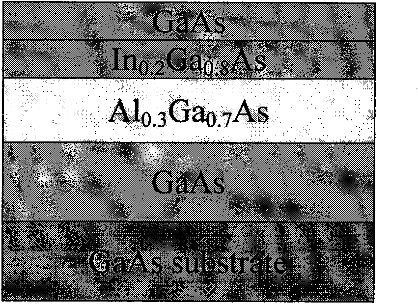
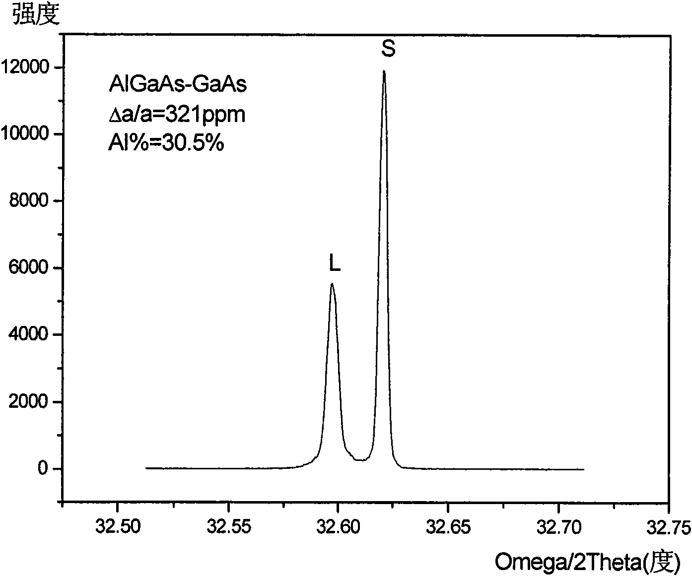
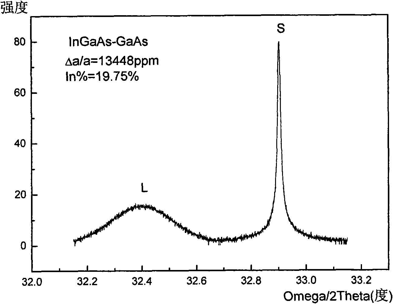
[0030] The material was grown on the semi-insulating single-throw GaAs(100) substrate by gas source molecular beam epitaxy, and the substrate temperature was 580°C. First, a 300nm GaAs buffer layer is epitaxially grown on the GaAs substrate, and a 1.6μm AlGaAs material is grown as a corrosion sacrificial layer. A 6nm InGaAs strained layer is grown on the corrosion sacrificial layer, and a 6nm GaAs inner tube wall is grown on the strained InGaAs material layer. material growth. pass figure 2 and image 3 According to the x-ray test analysis, the AlGaAs corrosion layer material and the InGaAs strain layer material composition meet the design requirements, and the material quality is very good.

[0031] The specific process is as follows:

[0032] (1) Send the GaAs(100) substrate into the pretreatment chamber of the gas source molecular beam epitaxy system GSMBE, and degas at 400-450°C for 25-35 minutes;

[0033](2) Transfer the above substrate to the growth chamber of GSMBE...


PUM

PropertyMeasurementUnit
thicknessaaaaaaaaaa
thicknessaaaaaaaaaa
thicknessaaaaaaaaaa

Abstract

The invention relates to a method for preparing III-V compound semiconductor nanotube structure material by GSMBE, which comprises the following steps: pretreating a substrate in a GSMBE system; using As2 obtained by arsine decomposition as an As source, adjusting the pressure PV of AsH3 in an air source furnace to 450 to 700 Torr, and controlling the intensity of molecular flows; transferring the substrate to a GSMBE growth chamber for epitaxial growth; and making patterns by using a semiconductor etching process, and making the III-V compound semiconductor nanotube structure material after etching. The III-V compound semiconductor material system is highly selective, convenient in resource as well as capable of doping nanotube interior and exterior wall materials. The preparation method is simple in operation, low in cost and suitable for large-scale production.

Description

technical field [0001] The invention belongs to the field of preparation of III-V compound semiconductor materials, in particular to a method for preparing III-V compound semiconductor nanotube structure materials by GSMBE (gas source molecular beam epitaxy). Background technique [0002] Semiconductor nanotubes are a new type of nanomaterials due to their special properties such as size effect, surface and interface, and electronic coherence in nanosystems. It has received great attention from the fields of physics, chemistry, materials science and many high-tech industries. Nanomaterials and nanotube structures have potential applications in the fields of manufacturing, information technology, energy, environment, health care, biotechnology, and national security. Compound semiconductor nanotubes can exhibit obvious quantum effects, and have good application prospects in the fields of infrared imaging, infrared lasers, semiconductor infrared detection, photoresistors, sol...

Claims


Application Information

Patent Timeline
Patent Type & Authority Applications(China)
IPC IPC(8): C30B29/40C30B25/02H01L21/205
Inventor 艾立鹍徐安怀孙浩齐鸣朱福英
Owner SHANGHAI INST OF MICROSYSTEM & INFORMATION TECH CHINESE ACAD OF SCI
Why Eureka
Try Eureka