Method for making high precision nanometer holes and nanometer hole arrays by utilizing focusing electronic beams
A technology of focusing electron beams and nanohole arrays, applied in nanotechnology, nanotechnology, nanostructure manufacturing, etc., can solve the problems of uncontrollable size and position of nanoholes, and achieve the effect of large application value and high efficiency
- Summary
- Abstract
- Description
- Claims
- Application Information
AI Technical Summary
Problems solved by technology
Method used
Image
Examples
Embodiment 1 1
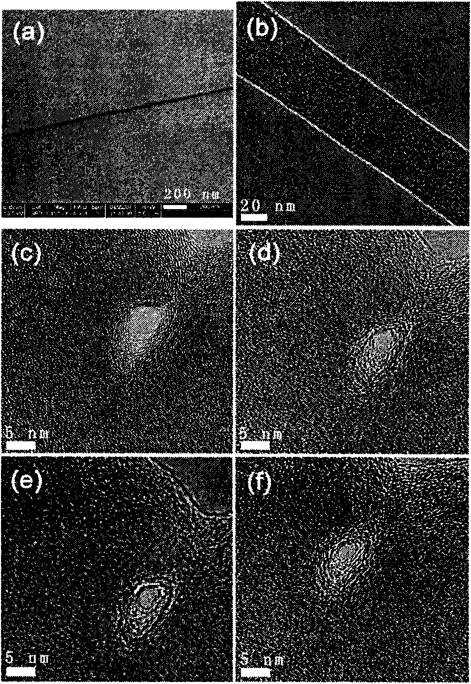
[0025] Embodiment 1, the preparation of 1nm diameter nanopore
[0026] (1) Preparation of polymethyl methacrylate fiber
[0027] Prepare the nanofiber of PMMA with electrospinning method: PMMA is dissolved in the mixed solution of chlorobenzene and DMF (chlorobenzene and DMF mix with the volume ratio of 1: 1), the operating voltage of electrospinning is 25kV, working distance ( Under the condition that the distance between the substrate and the needle head) is 12 cm, the fiber is deposited on the micro-grid, and the diameter of the obtained nanofiber is between 2 and 50 nanometers. To remove the solvent, the prepared PMMA nanofibers were heated at 50 °C for 30 min.
[0028] (2) Preparation of 1nm diameter nanopores
[0029] The PMMA nanofibers were placed in the sample stage of the high-resolution transmission electron microscope, and the vacuum degree was 10 -8 Torr, at room temperature, under the condition of working voltage of 200kV, adjust the diameter of the focused el...
Embodiment 2
[0031] Example 2. Preparation of nanopores with a diameter of 2nm
[0032] (1) Preparation of polymethyl methacrylate fiber
[0033] Same as embodiment one.
[0034] (2) Preparation of nanopores with a diameter of 2nm
[0035] The PMMA nanofibers were placed in the sample stage of the high-resolution transmission electron microscope, and the vacuum degree was 10 -8 Torr, at room temperature, under the condition of working voltage of 200kV, adjust the diameter of the focused electron beam to 0.5nm, and the intensity of the focused electron beam is 5×10 7 e / nm 2 s, the irradiation time is 20s.
[0036] The size of the nanopore is detected by high-resolution transmission electron microscopy: the diameter of the nanopore is 2nm.
Embodiment 3
[0037] Example 3, Preparation of Nanopores with a Diameter of 5nm
[0038] (1) Preparation of polymethyl methacrylate fiber
[0039] Same as embodiment one.
[0040] (2) Preparation of nanopores with a diameter of 5nm
[0041] The PMMA nanofibers were placed in the sample stage of the high-resolution transmission electron microscope, and the vacuum degree was 10 -8 Torr, at room temperature, under the condition of working voltage of 200kV, adjust the diameter of the focused electron beam to 0.5nm, and the intensity of the focused electron beam is 5×10 7 e / nm 2 s, the irradiation time is 60s.
[0042] The size of the nanopore is detected by high-resolution transmission electron microscopy: the diameter of the nanopore is 5 nm.
PUM
 Abstract
Description
Claims
Application Information

