Adhesive film for semiconductor, composite sheet, and method for producing semiconductor chip using them

A manufacturing method and semiconductor technology, which can be used in the manufacture of semiconductor/solid-state devices, semiconductor devices, and thin-film/sheet-like adhesives, etc. Fracture and other problems, to achieve the effect of suppressing chip cracks or burrs, excellent moisture resistance and reliability, and realizing processing speed

Inactive Publication Date: 2010-02-03
HITACHI CHEM CO LTD
View PDF2 Cites 5 Cited by
  • Summary
  • Abstract
  • Description
  • Claims
  • Application Information

AI Technical Summary

Problems solved by technology

However, in the case of the method of stretching the dicing tape to cut the semiconductor wafer after forming the modified portion on the semiconductor wafer by laser processing, it is difficult to completely break the adhesive film for semiconductors only by stretching the dicing tape. , it can be seen that it is actually difficult to obtain a semiconductor chip with a high yield rate
[0013] In addition, in the method of using a laminate in which grooves are formed or the method of using stealth dicing, although the adhesive film is easily broken by including a large amount of filler in the adhesive film, the generation of burrs can be suppressed to a certain extent. , but in this case there is a problem that it is difficult to attach the adhesive film to the semiconductor wafer at low temperature

Method used


Image

  • Adhesive film for semiconductor, composite sheet, and method for producing semiconductor chip using them
  • Adhesive film for semiconductor, composite sheet, and method for producing semiconductor chip using them
  • Adhesive film for semiconductor, composite sheet, and method for producing semiconductor chip using them

Examples


no. 1 approach

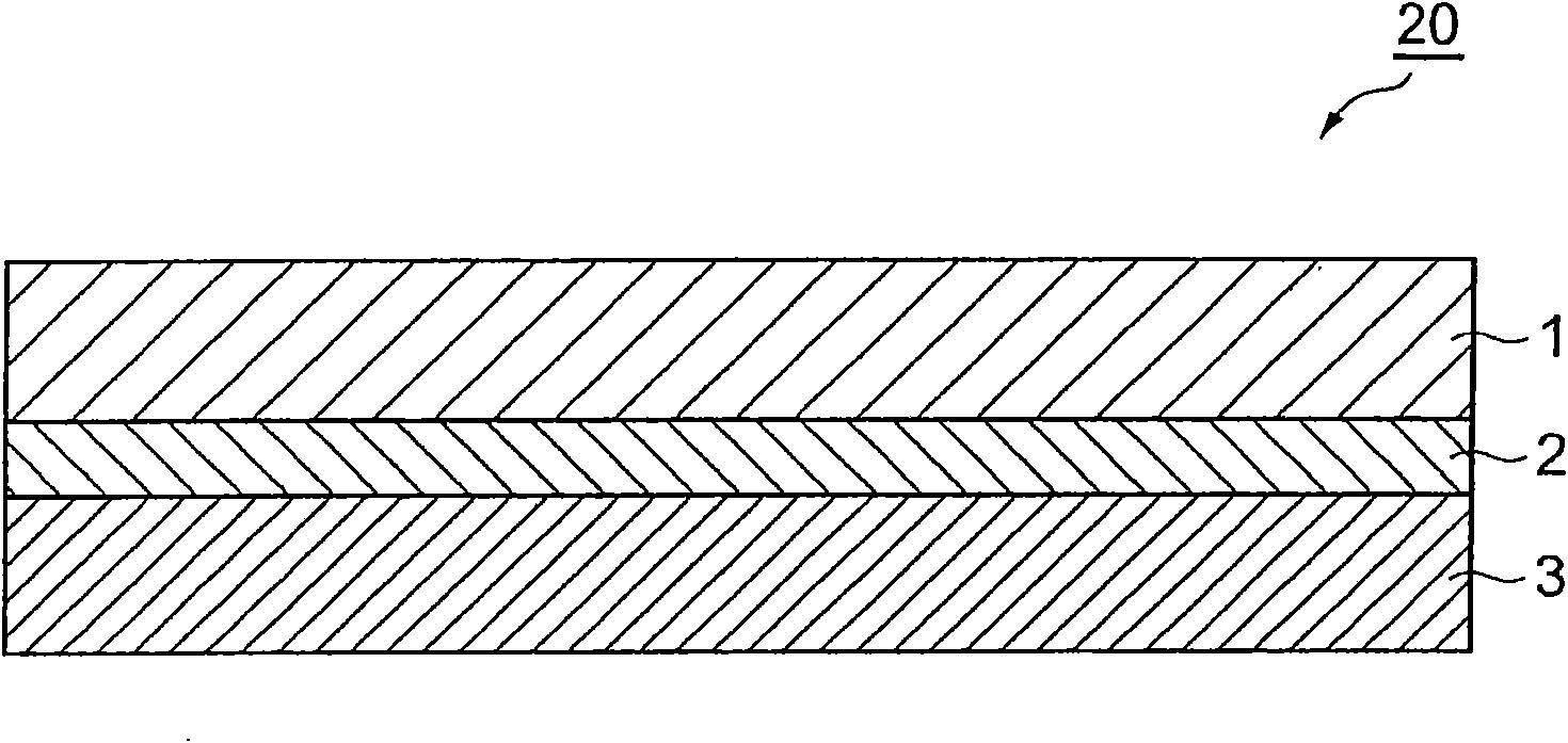
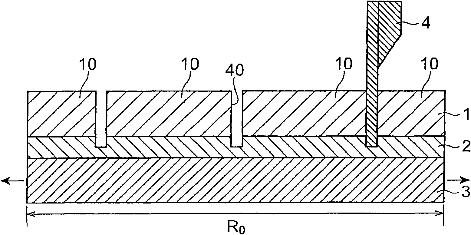
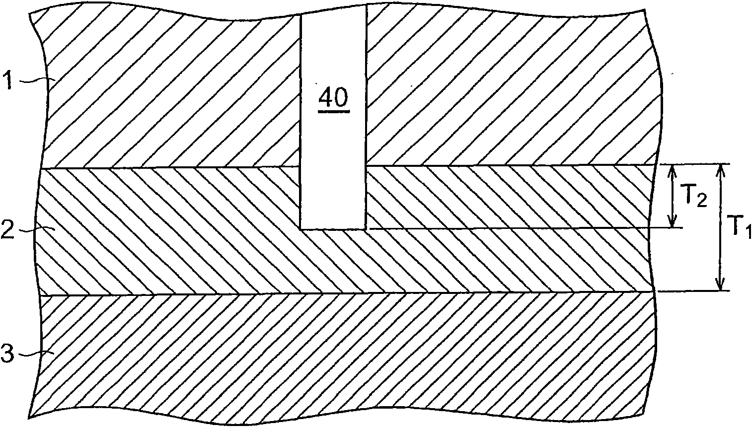
[0103] figure 1 , 2 , 3, 4 and 5 are cross-sectional views showing the method of manufacturing the semiconductor chip according to the first embodiment. The manufacturing method of the semiconductor chip of this embodiment includes: the process of preparing the laminated body 20 which laminated|stacked the semiconductor wafer 1, the adhesive film 2 for semiconductors, and the dicing tape 3 sequentially ( figure 1 ); the process of forming a groove 40 in the stacked body 20 from the semiconductor wafer 1 side ( figure 2 , 3 ); the process of dividing the adhesive film 2 for semiconductors along the slit 40 ( Figure 4 ); the process of picking up the semiconductor chip 10 together with the semiconductor adhesive film 2 ( Figure 5 ). The adhesive film for a semiconductor of the embodiment described above is used as the adhesive film 2 for a semiconductor.

[0104] figure 1 The laminated body 20 of the semiconductor wafer 1 is prepared by the following method, that is, t...

no. 2 approach

[0113] Image 6 , 7 , 8 and 9 are cross-sectional views showing the method of manufacturing the semiconductor chip according to the second embodiment. The method of this embodiment has: the process of preparing the laminated body 20 which laminated|stacked the semiconductor wafer 1, the adhesive film 2 for semiconductors, and the dicing tape 3 sequentially ( Figure 6-8 ); the process of dividing the semiconductor wafer 1 into a plurality of semiconductor chips 10 and dividing the adhesive film 2 for semiconductors by stretching the dicing tape 3 in a direction in which the plurality of semiconductor chips 10 are separated from each other ( Figure 9 ); a step of picking up the semiconductor chip 10 together with the adhesive film 2 for a semiconductor.

[0114] The process of preparing the laminated body 20 includes forming the modified portion 1a inside the semiconductor wafer 1 along the line 50 (hereinafter referred to as "planning line for dividing") that divides the se...

Embodiment 1

[0130] In a 500ml four-neck flask with a thermometer, a stirrer and a calcium chloride tube, add 1,3-bis(3-aminopropyl)tetramethyldisiloxane (0.1mol) as a diamine and as a solvent 150 g of N-methyl-2-pyrrolidone was stirred at 60°C. After dissolving the diamine, add 1,10-(decamethylene)bis(trimellitic dianhydride) (0.02mol) and 4,4'-oxydiphthalic anhydride (0.08mol) little by little , reacted at 60°C for 3 hours. Thereafter, after blowing N 2 While heating at 170° C., water in the system was removed together with a part of the solvent by azeotropy over 3 hours. The NMP solution of the polyimide resin obtained by removing water was used for preparation of an adhesive film.

[0131] In the NMP solution (containing 100 parts by weight of polyimide resin) of the polyimide resin obtained by utilizing the above operation, add 4 parts by weight of cresol novolac epoxy resin (made by Tohto Chemical Industry), 4,4'- [1-[4-[1-(4-Hydroxyphenyl)-1-methylethyl]phenyl]ethylene]bisphenol...


PUM

PropertyMeasurementUnit
Lengthaaaaaaaaaa

Abstract

There is provided an adhesive film for a semiconductor, which can be attached to a semiconductor wafer at low temperature and which allows semiconductor chips to be obtained at high yield from the semiconductor wafer while sufficiently inhibiting generation of chip cracks and burrs. The adhesive film for a semiconductor comprises a polyimide resin that can be obtained by reaction between a tetracarboxylic dianhydride containing 4,4'-oxydiphthalic dianhydride represented by chemical formula (I) below and a diamine containing a siloxanediamine represented by the following general formula (II) below, and that can be attached to a semiconductor wafer at 100 DEG C or below.

Description

technical field [0001] This invention relates to the manufacturing method of the adhesive film for semiconductors, a composite sheet, and the semiconductor chip using them. Background technique [0002] When mounting a semiconductor chip on a support member, silver paste has been mainly used conventionally as a die bonding material for bonding the semiconductor chip and the support member. However, with the miniaturization and high performance of semiconductor chips and the miniaturization and precision of supporting members used, in the method of using silver paste, there are wire bonding ( The problems such as the occurrence of poor conditions during wire bonding) are becoming more and more obvious. For this reason, in recent years, an adhesive film (adhesive film for a semiconductor) has been used instead of a silver paste. [0003] As a method of obtaining a semiconductor device using an adhesive film, there are a single-chip bonding method and a wafer backside bonding...

Claims


Application Information

Patent Timeline
IPC IPC(8): H01L21/301C09J7/00C09J179/08C09J183/10H01L21/52
CPCH01L2224/29191H01L2924/10253
Inventor 中村祐树北胜勉片山阳二畠山惠一
Owner HITACHI CHEM CO LTD
Why Eureka
Try Eureka