Nano-pore electric sensor

A nanopore and sensor technology, applied in the field of sensors, can solve problems such as integration of nanometer electrodes with single base resolution, and achieve the effect of rapid electronic gene sequencing and simple method.

Active Publication Date: 2010-04-14
ZHEJIANG UNIV
View PDF0 Cites 49 Cited by
  • Summary
  • Abstract
  • Description
  • Claims
  • Application Information

AI Technical Summary

Problems solved by technology

However, although the current technology for preparing nanopores is relatively mature [J.Li, et al, Nature 2001, 412, 166-169; A.J.Storm, et al, Nature Mater.2003, 2, 537-540; M.J.Kim, et al , Adv.Mater.2006, 18, 3149-3153; B.M.Venkatesan, et al, Adv.Mater.2009, 21, 2771-2776.], however, so far there is no technical method to combine nanoelectrodes with single-base resolution Integrated in nanopore system

Method used


Image

  • Nano-pore electric sensor
  • Nano-pore electric sensor
  • Nano-pore electric sensor

Examples


Embodiment 1

[0021] Embodiment 1: Chemical vapor deposition method prepares and transfers graphene

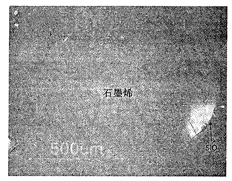
[0022] In SiO 2 (300nm) / Si(500μm) prepared 100nm Cu film, placed in ultra-high vacuum (5.0×10 -9 torr) heat treatment at 950°C for 30 minutes; then, through C 2 h 4 Gas growth for 60 seconds; thereby obtaining graphene on the Cu film. Transfer graphene from Cu to SiO 2 On / Si: spin-coat 500nm Polymethylmethacrylate (PMMA) layer on graphene, place the graphene / Cu that is coated with PMMA in iron nitrate solution and corrode Cu film, thereby obtain PMMA / graphene, then PMMA / graphite ene transfer to SiO 2 / Si on ( image 3 and Figure 4), and finally, use acetone to dissolve PMMA, so that graphene is transferred to SiO 2 / Si on.

[0023] Effect: High-uniform single-layer graphene can be prepared on the surface of metal Cu, and it is easy to transfer graphene to the insulating layer by corroding the Cu catalytic layer.

Embodiment 2

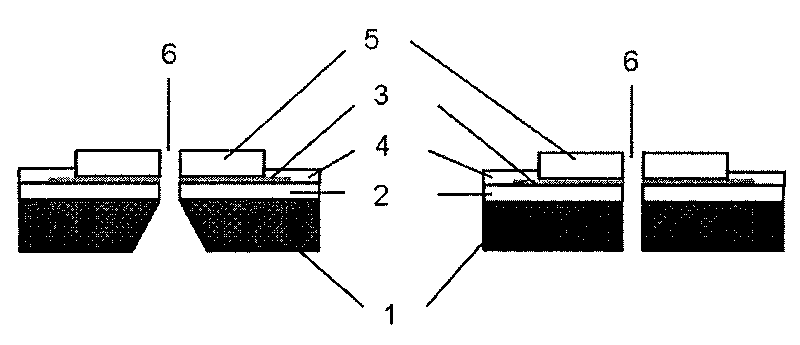
[0025] like Figure 5 Shown: on a 500μm thick monocrystalline silicon substrate 1( Figure 5 a) Preparation of 50nm SiO by upper thermal oxidation 2 Insulation layer 2 ( Figure 5 b); the prepared graphene layer 7 is transferred to SiO 2 Insulation layer 2 ( Figure 5 c); Graphene can be prepared by different methods, such as chemical vapor deposition on metallic Cu, and then transferred onto SiO 2 insulating layer2. Graphene electrode pair 3 patterns were prepared by photolithography and oxygen plasma etching ( Figure 5 d). Among them, since the thickness of the graphene electrode layer is only about 0.35nm, in order to establish effective electrical contact, on the graphene electrode pair 3 patterns, use photolithography and etching technology to prepare Cr(5nm) / Au on the graphene electrode pair. (50nm) electrical contact layer 4 ( Figure 5 e); Then, prepare 70nm Al by atomic layer deposition 2 o 3 and the preparation of 100nm Si by plasma-enhanced chemical vapor...

Embodiment 3

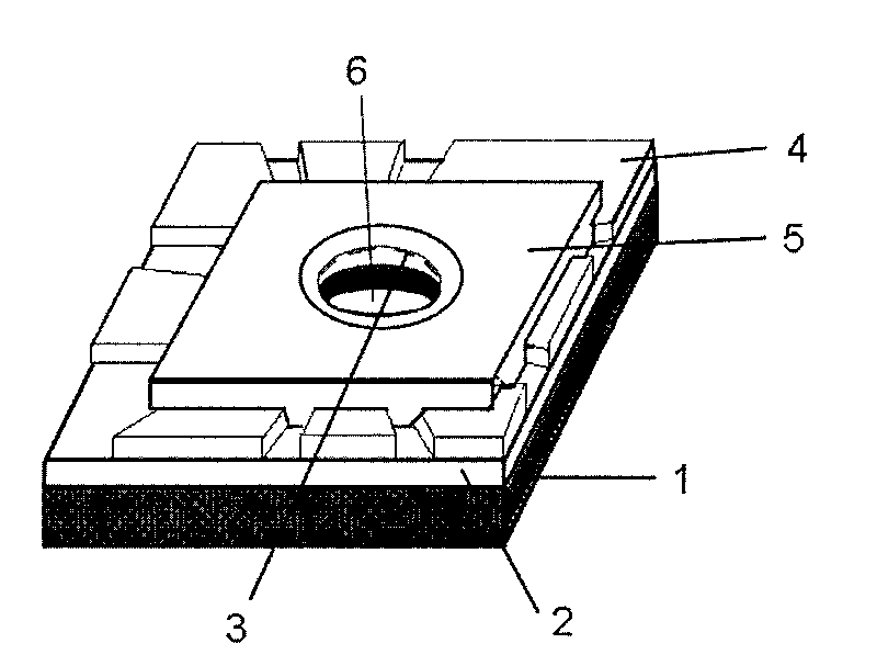
[0027] like Figure 6 Shown: On a 500 μm thick single crystal SiC {0001} substrate 1 in ultra-high vacuum (1.0 × 10 -10 torr) for thermal (950°C-1400°C) surface treatment to become Si-terminated surface or C-terminated surface insulating layer 2 ( Figure 6 a), thus epitaxial growth obtains graphene layer 7 ( Figure 6 b). Graphene electrode pair 3 patterns were prepared by photolithography and oxygen plasma etching ( Figure 6 c). Wherein, since the thickness of the graphene electrode layer is only about 0.7nm, in order to establish an effective electrical contact, photolithography and etching techniques are used to prepare Pd (50nm) electrodes on the graphene electrode pair 3 patterns. Contact layer 4 ( Figure 6 d); Then, prepare 100nm Si by plasma-enhanced chemical vapor deposition 3 N 4 Insulation layer 5( Figure 6 e); Finally, prepare a 3nm nanopore 6 ( Figure 6 f).

[0028] Effect: High-uniform graphene can be prepared on a large scale on an ultra-high vacuu...


PUM

PropertyMeasurementUnit
thicknessaaaaaaaaaa
pore sizeaaaaaaaaaa
thicknessaaaaaaaaaa

Abstract

The invention discloses a nano-pore electric sensor. The nano-pore electric sensor comprises a baseplate, first insulating layers, symmetrical electrodes, electric contact layers, second insulating layers and nano-pores. The first insulating layers and the symmetrical electrodes are sequentially arranged on the baseplate; the electric contact layers are arranged on the first insulating layers and the edges of the symmetrical electrodes; the second insulating layers are arranged on the symmetrical electrodes; and the nano-pores are arranged in the centers of the baseplate, the first insulating layers, the symmetrical electrodes and the second insulating layers. The thickness of each nano-electrode can be controlled within the range from 0.35 to 0.7nm to meet the requirement on resolution for detecting the electric character of a single base group in single-chain DNA, thereby being suitable for the low-cost and fast electronic gene sequence test. The nano-pore electric sensor solves the technical problem for integrating the nano-electrodes in the nano-pores, and the method for preparing the nano-electrodes is simple.

Description

technical field [0001] The invention relates to sensors, in particular to a nanopore electrical sensor. Background technique [0002] Nanopores can detect and characterize biomolecules such as DNA, RNA, and peptides at the single-molecule resolution level. Potential nanopore-based single-molecule gene sequencing technology does not require fluorescent markers or PCR reactions, and is expected to be able to directly and Quickly "read" the base sequence of DNA; this sequencing technology is expected to greatly reduce the cost of sequencing and realize personalized medicine [M.Zwolak, M.Di Ventra, Rev.Mod.Phys.2008, 80, 141-165; D. Branton, et al., Nature Biotechnol. 2008, 26, 1146-1153]. Nanopore-based single-molecule gene sequencing technology uses DNA bases to sequentially pass through nanopores under the action of electrophoresis, and at the same time detects the difference in optical or electrical signals generated when bases pass through nanopores to sequence DNA. Nanop...

Claims


Application Information

Patent Timeline
Patent Type & Authority Applications(China)
IPC IPC(8): G01N27/00
CPCG01N33/48721B82Y15/00C12Q1/6869C12Q2565/631
Inventor 徐明生陈红征施敏敏吴刚汪茫
Owner ZHEJIANG UNIV
Why Eureka
Try Eureka