Nanopore electrical sensor

A nanopore and sensor technology, applied in the field of sensors, to achieve the effect of avoiding pollution, simple method and firm structure

Active Publication Date: 2012-11-21
ZHEJIANG UNIV
View PDF2 Cites 0 Cited by
  • Summary
  • Abstract
  • Description
  • Claims
  • Application Information

AI Technical Summary

Problems solved by technology

The nano functional layer is sandwiched between the first insulating layer and the second insulating layer, and the periphery of the nanohole is in the shape of a whole piece, which solves the problem of different orientations that may exist when bases pass through the nanopore, and ensures that the four bases of DNA are compatible with each other. The most appropriate and different interactions exist in the nano-functional layer

Method used


Image

  • Nanopore electrical sensor
  • Nanopore electrical sensor
  • Nanopore electrical sensor

Examples


Embodiment 1

[0031] Graphene film was synthesized on Cu by chemical vapor deposition method: the surface of Cu sheet with a thickness of 25 μm was polished and cleaned, and then placed in an ultra-high vacuum (1.0×10 -9 torr) heat treatment at 900°C for 30 minutes; 2 h 4 The gas (10 Pa) was grown for 10 minutes; finally, the temperature was rapidly cooled to room temperature, so that a graphene film was obtained on the Cu sheet.

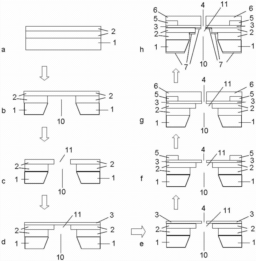
[0032] like figure 1 Shown: 50 nm SiO was sequentially fabricated on a 600 μm thick monocrystalline Si substrate 1 2 and 30 nm Si 3 N 4 Composite insulating layer 2 ( figure 1 a).

[0033] Using photolithography technology, and using KOH solution and buffered HF solution to etch the silicon substrate and SiO 2 And prepare a square opening 10 ( figure 1 b).

[0034] E-beam etching with SF 6 A hole 11 ( figure 1 c).

[0035] The prepared graphene film is transferred to the silicon nitride film as the nano-functional layer 3, and the graphene film ...

Embodiment 2

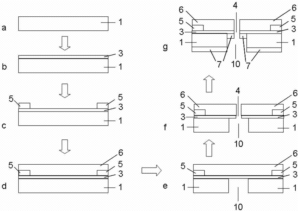
[0050] like image 3 Shown: On a 100 μm thick insulating single crystal SiC {0001} substrate 1 ( image 3 a) In ultra-high vacuum (1.0×10 -10 torr) is subjected to thermal (1000° C. to 1500° C.) surface treatment and epitaxial growth to obtain a graphene film layer 3 ( image 3 b).

[0051] Since the thickness of the graphene film nano-functional layer 3 is about 0.7 nm, in order to establish an effective electrical contact, a Pd (50 nm) electrical contact layer 5 is prepared on the edge of the graphene functional layer 3 using photolithography and etching techniques ( image 3 c).

[0052] Preparation of 50 nm Si by Low Pressure Chemical Vapor Deposition 3 N 4 The insulating layer is used as the second insulating layer 6, and it is polished and planarized ( image 3 d).

[0053] A hole 10 with a diameter of approximately 2.5 μm is prepared by electron beam etching and reactive particle beam etching of the SiC substrate 1 in a fluorinated gas ( image 3 e).

[0054]...

Embodiment 3

[0065] like Figure 4 Shown: 100 nm Si prepared on a 600 μm thick monocrystalline Si substrate 1 3 N 4 The first insulating layer 2 ( Figure 4 a); Si in the insulating layer 3 N 4 A 100 nm metallic Ni catalytic layer 12 was prepared on it ( Figure 4 b), the metal catalytic layer 12 is used to grow the BNC nano functional layer 3 ( Figure 4 c).

[0066] After preparing a 100 nm metallic Ni catalytic layer 12, a BNC layered film was prepared as a nanofunctional layer 3 by chemical vapor deposition: it was placed in an ultra-high vacuum (1×10 -8 torr), then in Ar / H 2 atmosphere ( ~ 20vol%H 2 ) heat treatment at 750°C for about 120 minutes, then raise the temperature to 950°C for 30 minutes; turn off the Ar / H 2 , and changed to methane and ammonia to synthesize BNC film, the growth time is 20 minutes, and its thickness is about 0.7 nm.

[0067] After BNC nano functional layer 3 is synthesized, put it in 1M FeCl 3 Metal Ni catalytic layer 12 is reacted in solution, ...


PUM

PropertyMeasurementUnit
thicknessaaaaaaaaaa
pore sizeaaaaaaaaaa
thicknessaaaaaaaaaa

Abstract

The invention discloses a nanopore electrical sensor, which comprises a substrate, a first insulation layer, a nano functional layer, an electrical contact layer, a second insulation layer and nanopores, wherein the first insulation layer and the nano functional layer are formed on the substrate in turn; the electrical contact layer is formed on the first insulation layer and on the edge of the nano functional layer; and the second insulation layer is formed on the nano functional layer; and nanopores are formed in the centers of the substrate, the first insulation layer, the nano functional layer and the second insulation layer. The thickness of the nano functional layer of the nanopore electrical sensor can be kept between 0.3 and 0.7 nanometers and meets the requirements for detecting the resolution of the electrical characteristics of single basic groups in a single-chain DNA, so the nanopore electrical sensor is suitable for convenient and quick electronic gene sequencing. The nanopore electrical sensor disclosed by the invention solves the technical problem of integrating the nano functional layer in nano pores, and the method for preparing the nano functional layer is simple; and the mutual influences between the basic groups and the nano functional layer, which are generated due to the possible different orientation of the basic groups of the DNA passing through the nano pores, are eliminated.

Description

technical field [0001] The invention relates to sensors, in particular to a nanopore electrical sensor. Background technique [0002] Nanopores can detect and characterize biomolecules such as DNA, RNA, and peptides at the single-molecule resolution level. Potential nanopore-based single-molecule gene sequencing technology does not require fluorescent markers or PCR reactions, and is expected to be able to directly and Quickly "read" the base sequence of DNA; this sequencing technology is expected to greatly reduce the cost of sequencing and realize personalized medicine. Nanopore-based single-molecule gene sequencing technology mainly has three detection methods: Strand-sequencing using ionic current blockage, Strand-sequencing using transverse electron currents, Optical information (Nanopore sequencing using synthetic DNA and optical readout). The depth of the nanopores currently prepared is generally greater than 10 nm, which is far beyond the base distance of single-st...

Claims


Application Information

Patent Timeline
Patent Type & Authority Patents(China)
IPC IPC(8): G01N27/00C12M1/34B82B1/00
Inventor 徐明生陈红征施敏敏吴刚汪茫
Owner ZHEJIANG UNIV
Why Eureka
Try Eureka