Packaging structure and packaging method of semiconductor device
A device packaging and semiconductor technology, applied in the direction of semiconductor devices, semiconductor/solid-state device manufacturing, semiconductor/solid-state device components, etc., can solve problems such as exceeding, significant thermo-mechanical stress, and increasing process cost, etc., to achieve thermo-mechanical stress reduction Small, avoid thermal mismatch, improve the effect of electrical performance
- Summary
- Abstract
- Description
- Claims
- Application Information
AI Technical Summary
Problems solved by technology
Method used
Image

Examples
Embodiment Construction
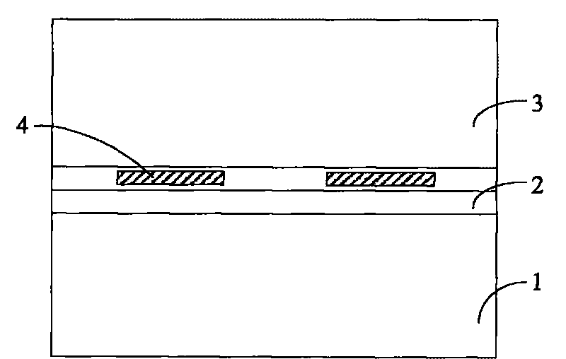
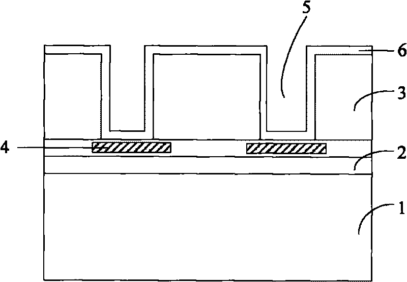
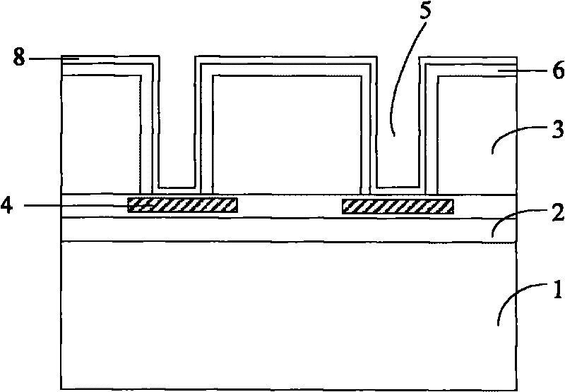
[0029] At present, the process method of processing through-silicon via interconnection structure is: (1) using reactive ion etching-inductively coupled plasma (RIE-ICP) method to etch to form through holes on the chip; (2) using chemical vapor deposition (CVD ) Oxide or nitride passivation method forms a dielectric layer (usually silicon dioxide) on the inner wall of the through hole; (3) metallizes the through hole; (4) backside grinding of the wafer.
[0030] This process flow has the following problems: (1) There is only a very thin dielectric layer (usually silicon dioxide) between the chip and the conductor layer, which results in a high capacitance between the TSV interconnects, Sometimes it even exceeds the capacitance value of the standard wire bonding interconnection method; (2) The conductor layer of predetermined thickness is filled in the via hole, due to the large thermal mismatch between the silicon and the conductor layer, this will cause the thermal cycle (3) ...
PUM
| Property | Measurement | Unit |
|---|---|---|
| Opening size | aaaaa | aaaaa |
| Thickness | aaaaa | aaaaa |
| Thickness | aaaaa | aaaaa |
Abstract
Description
Claims
Application Information
 - R&D
- Intellectual Property
- Life Sciences
- Materials
- Tech Scout
- Unparalleled Data Quality
- Higher Quality Content
- 60% Fewer Hallucinations
Browse by: Latest US Patents, China's latest patents, Technical Efficacy Thesaurus, Application Domain, Technology Topic, Popular Technical Reports.
© 2025 PatSnap. All rights reserved.Legal|Privacy policy|Modern Slavery Act Transparency Statement|Sitemap|About US| Contact US: help@patsnap.com