Packaging structure and packaging method of semiconductor device

A device packaging and semiconductor technology, applied in the direction of semiconductor devices, semiconductor/solid-state device manufacturing, semiconductor/solid-state device components, etc., can solve the problems of significant thermo-mechanical stress, increase the cost of process methods, exceed, etc., and achieve thermo-mechanical stress reduction Small, avoid thermal mismatch, improve the effect of electrical performance

Active Publication Date: 2011-09-14
CHINA WAFER LEVEL CSP
View PDF1 Cites 0 Cited by
  • Summary
  • Abstract
  • Description
  • Claims
  • Application Information

AI Technical Summary

Problems solved by technology

[0010] This process flow can effectively realize high-density three-dimensional through-hole interconnection, but there are the following problems: (1) there is only a very thin dielectric layer (usually silicon dioxide) between the chip and the conductor layer, This leads to the formation of high capacitance between TSV interconnections, sometimes even exceeding the capacitance value of the standard wire bonding interconnection; (2) The conductive layer of predetermined thickness is filled in the via hole, due to the gap between the silicon and the conductive layer Large thermal mismatch between them, which will cause significant thermomechanical stress during thermal cycling; (3) It takes a long time to form a conductive layer in the through hole by electroplating, which increases the cost of the process method

Method used


Image

  • Packaging structure and packaging method of semiconductor device
  • Packaging structure and packaging method of semiconductor device
  • Packaging structure and packaging method of semiconductor device

Examples


Embodiment Construction

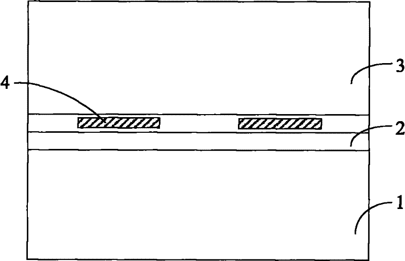
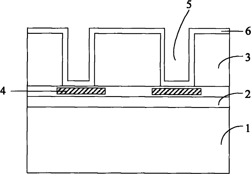
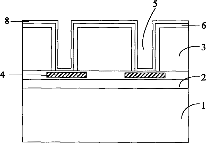
[0029] The current process methods for processing the through-silicon via interconnect structure are: (1) using reactive ion etching-inductively coupled plasma (RIE-ICP) method to etch through holes on the chip; (2) using chemical vapor deposition (CVD) (1) Oxide or nitride passivation method to form a dielectric layer (usually silicon dioxide) on the inner wall of the through hole; (3) metallize the through hole; (4) back-grind the wafer.

[0030] This process has the following problems: (1) There is only a very thin dielectric layer (usually silicon dioxide) between the chip and the conductor layer, which leads to the formation of high capacitance between TSV interconnects. Sometimes it even exceeds the capacitance value of the standard wire bonding interconnection method; (2) A conductor layer with a predetermined thickness is filled in the through hole. Due to the large thermal mismatch between the silicon and the conductor layer, it will be in the thermal cycle process. (3) ...


PUM


Abstract

The invention discloses a packaging structure and a packaging method of a semiconductor device. The packaging structure of the semiconductor comprises a chip, a passivation layer positioned above the chip, a pad positioned above the passivation layer, a first through hole running through the chip and the passivation layer along a thickness direction to the outside of the pad, a seed crystal layerpositioned in the inner wall of the first through hole, a conductor layer positioned on the seed crystal layer, a conductive layer filling up the first through hole, a second through hole, an insulating medium layer, a convex point lower metal layer and convex points, wherein the seed crystal layer, the conductor layer and the conductive layer in the first hole form a first conductive plug; the second through hole runs through the chip and the passivation layer along the thickness direction to the outside of the pad, is positioned around the first through hole and shares a side wall with the first through hole; the insulating medium layer is positioned above the chip, fills up the second through hole and is exposed out of the first conductive plug; the convex point lower metal layer is positioned on the insulating medium layer on the first conductive plug and the periphery of the conductive plug; and the convex points are on the convex point lower metal layer. In the packaging structure and the packaging method, ultra high capacitance caused by TSV interconnection is avoided and the electrical property of the semiconductor packaging structure is improved.

Description

Technical field [0001] The invention relates to the field of semiconductor packaging, in particular to a semiconductor device packaging structure and a packaging method thereof. Background technique [0002] Wafer Level Chip Size Packaging (WLCSP) technology is a technology in which the entire wafer is packaged and tested and then cut to obtain a single finished chip. The packaged chip size is consistent with the bare chip. Wafer-level chip size packaging technology changes the traditional packaging such as ceramic leadless chip carrier (Ceramic Leadless Chip Carrier), organic leadless chip carrier (Organic Leadless Chip Carrier) and digital camera module mode, conforming to the market's demand for microelectronic products Increasingly light, small, short, thin and low price requirements. The chip size after wafer-level chip size packaging technology has reached a high degree of miniaturization, and the chip cost has been significantly reduced as the chip size decreases and the ...

Claims


Application Information

Patent Timeline
Patent Type & Authority Patents(China)
IPC IPC(8): H01L23/485H01L23/528H01L23/532H01L21/50H01L21/60H01L21/768
CPCH01L2224/10
Inventor 王宥军王之奇俞国庆邹秋红王蔚
Owner CHINA WAFER LEVEL CSP
Why Eureka
Try Eureka