Method for preparing tri-dimension-limited crystal-facet-dependent silicon nanostructures

A silicon nano and three-dimensional technology, applied in the fields of nanostructure manufacturing, nanotechnology, nanotechnology, etc., can solve problems such as unfavorable large-scale integration of devices, increased device power consumption, and increased device resistance, etc. device resistance, the effect of overcoming inconsistencies

Inactive Publication Date: 2010-06-09
INST OF SEMICONDUCTORS - CHINESE ACAD OF SCI
View PDF0 Cites 8 Cited by
  • Summary
  • Abstract
  • Description
  • Claims
  • Application Information

AI Technical Summary

Problems solved by technology

[0006] However, due to the adoption of top-layer silicon thinning technology, the thickness of the top-layer silicon except the area where the nanostructure is located is only 20-50 nanometers, which brings great difficulties to the

Method used


Image

  • Method for preparing tri-dimension-limited crystal-facet-dependent silicon nanostructures
  • Method for preparing tri-dimension-limited crystal-facet-dependent silicon nanostructures
  • Method for preparing tri-dimension-limited crystal-facet-dependent silicon nanostructures

Examples


preparation example Construction

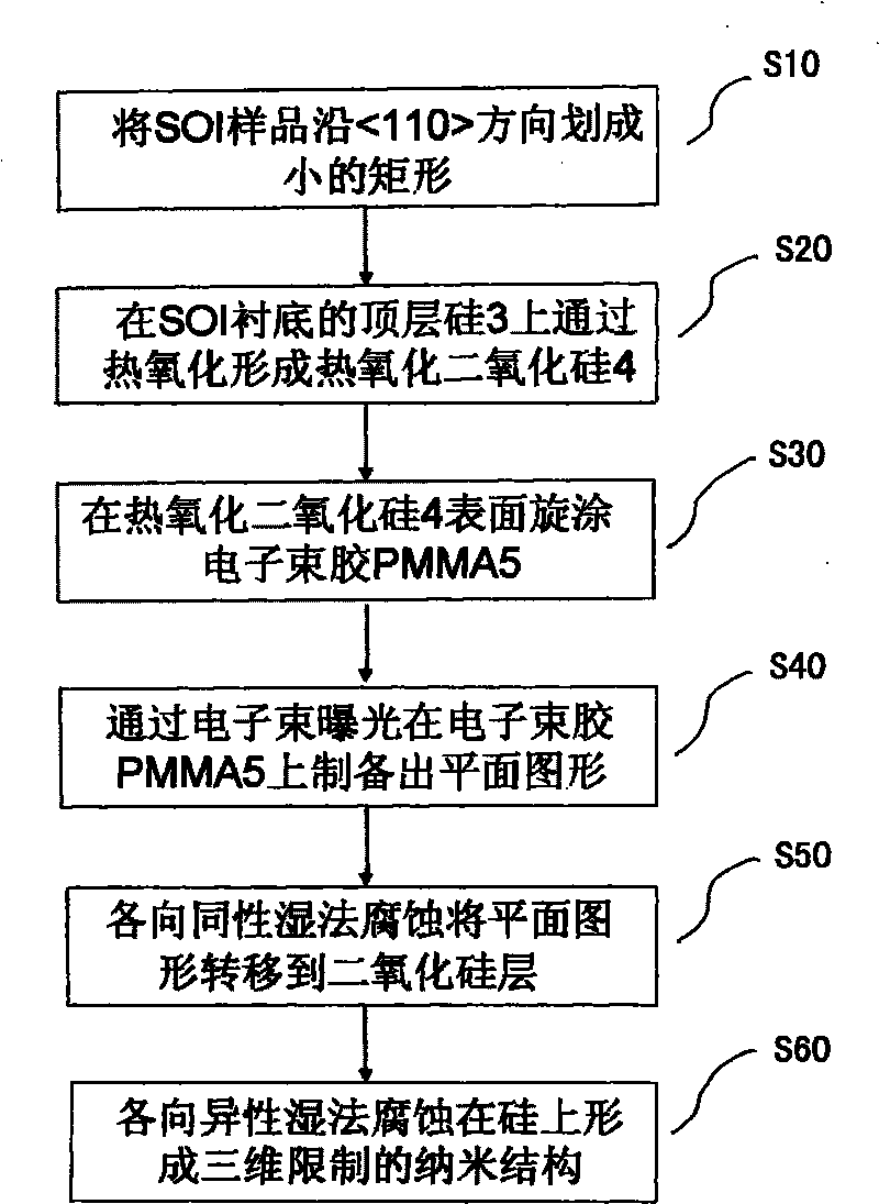
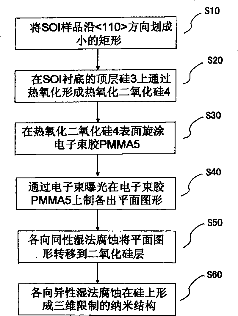
[0030] see figure 2 , figure 2 Shown is a flow chart of making a three-dimensional confined silicon nanostructure dependent on a crystal plane. A method for preparing a three-dimensional confined silicon nanostructure dependent on a crystal plane in the present invention comprises the following steps:

[0031] Step S10: using silicon-on-insulator as the substrate, and the crystal plane orientation of the top layer silicon of the silicon-on-insulator material is (100);

[0032] Step S20: Carry out scribing on the substrate along the crystal direction, as a reference direction during exposure;

[0033] Step S30: performing thermal oxidation on the substrate to form a silicon dioxide mask layer;

[0034] Step S40: Using electron beam exposure to generate a planar pattern, the electron beam exposure uses positive electron beam glue PMMA as a resist, and the planar pattern generated by electron beam exposure is based on the nanowire pattern There are openings at both ends of ...

Embodiment

[0039] based on figure 2 The flow chart for preparing a three-dimensional confinement silicon nanostructure dependent on crystal planes is shown, and the method for preparing a three-dimensional confinement silicon nanostructure dependent on crystal planes of the present invention will be further described in detail below in conjunction with specific examples.

Embodiment approach

[0040]A kind of process implementation method utilizing electron beam exposure provided by the present invention, specifically comprises the following steps:

[0041] (1) Determine the reference direction during electron beam exposure: Since the marking edge of the (100) oriented SOI substrate is along the crystal direction, it can be used as a reference edge for scribing. In the subsequent electron beam exposure process , which is further used as a reference direction during electron beam exposure;

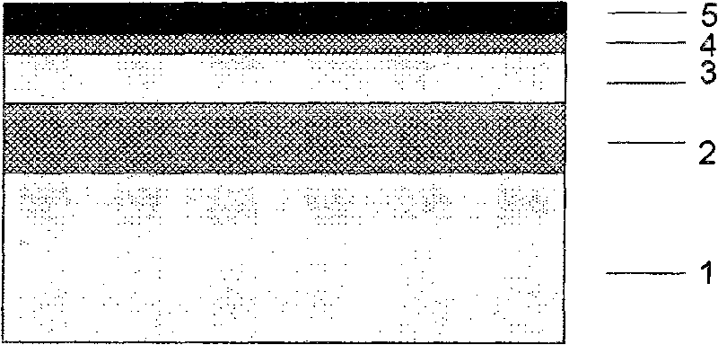
[0042] (2) thermal oxidation: yes figure 1 The top layer of silicon 3 on the SOI substrate shown in is thermally oxidized to form a 20nm thick silicon dioxide mask layer 4 on the surface of the top layer of silicon 3, and the thermally oxidized silicon dioxide of this layer is used as Masking layers for anisotropic wet etching.

[0043] (3) spin-coated electron beam glue: in figure 1 Spin-coat a layer of electron beam glue 5PMMA EL4 on the surface of the thermally oxidized si...


PUM


Abstract

The invention provides a method for preparing a tri-dimension-limited crystal-facet-dependent silicon nanostructure, which is characterized by comprising the following steps: (a) taking silicon-on-insulator (SOI) as a substrate; (b) scribing on the substrate along the crystal orientation (110) as a reference direction for exposure; (c) performing heat oxidation on the substrate to generate a silica mask layer; (d) adopting electron-beam exposure to generate a plane figure; (e) eroding the silica mask layer by using isotropic corrosive liquids; and (f) obtaining the tri-dimension-limited crystal-facet-dependent silicon nanostructure on the silicon layer below the silica mask layer by using isotropic wet corrosion.

Description

technical field [0001] The invention relates to the field of semiconductor micro-nano processing in nanoelectronics technology, in particular to a manufacturing process that combines electron beam exposure and silicon anisotropic wet etching to form a (100)-oriented silicon-on-insulator (SOI) substrate A processing method for preparing three-dimensional confined silicon nanostructures dependent on crystal planes that can be applied to quantum devices Background technique [0002] Nanoelectronics technology is the most important branch of nanotechnology. The main research content of nanoelectronics technology is the processing of nanostructures with characteristic sizes in the range of 0.1-100 nanometers and the research and development of electronic devices with quantum effects. Traditional quantum devices only use the particle nature in the wave-particle duality of electrons, and realize signal processing by controlling the number of electrons. With the improvement of inte...

Claims


Application Information

Patent Timeline
IPC IPC(8): B82B3/00
Inventor 杨香韩伟华王颖张杨杨富华
Owner INST OF SEMICONDUCTORS - CHINESE ACAD OF SCI
Why Eureka
Try Eureka