Growth process for N-type solar energy silicon single crystal with minority carrier service life of larger than or equal to 1,000 microseconds

A silicon single crystal, N-type technology, which is applied in the field of growing N-type silicon single crystals by the Czochralski method, can solve the problems of low service life of N-type Czochralski silicon single crystals, and achieve the effects of low cost, low service life and high efficiency

Inactive Publication Date: 2010-06-09
任丙彦 +1
View PDF3 Cites 24 Cited by
  • Summary
  • Abstract
  • Description
  • Claims
  • Application Information

AI Technical Summary

Problems solved by technology

[0004] The purpose of the present invention is to provide an N-type solar silicon single crystal growth process with a minority carrier lifetime greater than or equal to 1000 microseconds. The Czochralski method is used to grow N-type high-life silicon single crystals, which can solve the problem of low lifetime of N-type Czochralski silicon single crystals. problem

Method used


Image

  • Growth process for N-type solar energy silicon single crystal with minority carrier service life of larger than or equal to 1,000 microseconds
  • Growth process for N-type solar energy silicon single crystal with minority carrier service life of larger than or equal to 1,000 microseconds
  • Growth process for N-type solar energy silicon single crystal with minority carrier service life of larger than or equal to 1,000 microseconds

Examples


Embodiment 1

[0021] Manufacture 6-inch single crystal according to the present invention

[0022] The present invention uses four-level bulk polysilicon (commercially available) for solar energy, phosphorus dopant (granular low-resistance phosphorus single crystal, low resistivity single crystal grown by Czochralski method, at room temperature, resistivity 0.001~0.005 Ω·cm). The resistivity measurement equipment is the HDY~4 four-probe tester produced by Guangzhou Semiconductor.

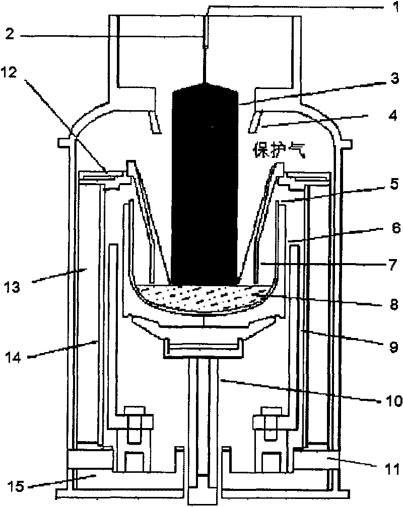
[0023] The structure of the monocrystalline silicon furnace that the present invention uses is as figure 1 As shown, 1~pulling; 2~seed crystal; 3~finished single crystal; 4~drain tube a; 5~quartz crucible; 6~graphite crucible; 7~drain tube b; 8~fused silicon; 9~ Heater; 10 ~ crucible rod; 11 ~ exhaust hole; 12 ~ upper cover; 13 ~ forming felt; 14 ~ heat preservation cylinder; 15 ~ heat preservation felt. Among them, 4 ~ guide tube a, 7 ~ guide tube b, 11 ~ exhaust holes are different from the disclosed convent...

Embodiment 2

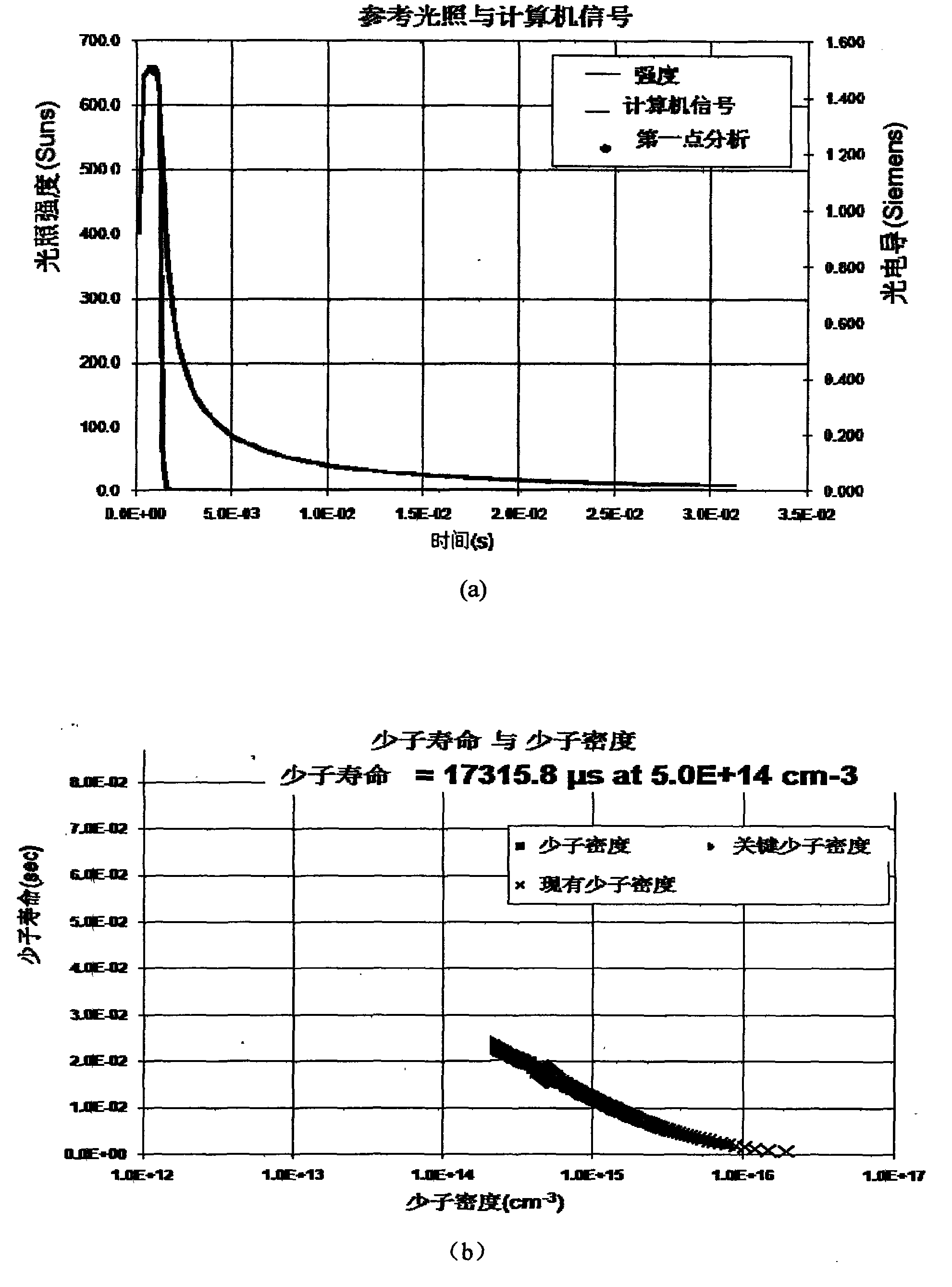
[0035] The second example of representative experimental results: Φ8" single crystal was prepared under the same process conditions.

[0036] Φ8″ grown under a Φ20″ thermal field device with a feeding capacity of 90 kg, N-type crystal orientation, the resistivity of the silicon single crystal rod, the head ρ≤20Ω·cm, the tail ρ≥1Ω·cm. The interstitial oxygen content is [Oi]≤17.5ppma, the replacement carbon content is [Cs]≤0.5ppma, and the non-equilibrium minority carrier lifetime τ≥1000μs.

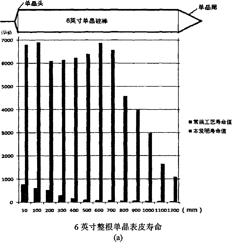
[0037] Minority life expectancy test results are as follows: figure 2 The shown (a) is the test condition of the minority carrier lifetime, (b) is the test result of the minority carrier lifetime; the life comparison of the Φ8″ single crystal obtained by the present invention and the conventional process (commonly used in the Czochralski silicon industry) is detailed in Figure 4 , (a) is the life comparison of the entire 8-inch single crystal skin, (b) is the center-to-edge life compari...


PUM

PropertyMeasurementUnit
electrical resistivityaaaaaaaaaa
charge carrier lifetimeaaaaaaaaaa

Abstract

The invention relates to a growth process for N-type solar energy silicon single crystal with minority carrier service life of larger than or equal to 1,000 microseconds. The appearance is in 6-8 inches, the (100) crystal orientation resistivity range is between 1 omega.cm and 20 omega.cm, the minority carrier service life of the surface and the section is larger than or equal to 1,000 microseconds, the clearance oxygen content [Oi] is smaller than or equal to 17.5ppma, and the substituted carbon content [Cs] is smaller than or equal to 0.5ppma. Phosphorus-doped block-shaped polycrystalline silicon is used as a raw material to prepare the N-type solar energy silicon single crystal. The process comprises the steps of: charging, heating, leading diameter, maintaining equal diameter, collecting, cooling, heating by a program, stably heating and melting the material; after a thermal field in melting silicon is stable, leading the thin diameter, lifting the tail part of a single crystal to the upper edge of a guide cylinder with the cooling time of not larger than three hours. The crystal growth process is practical, has high efficiency and low cost, can prepare the N-type single crystal silicon which is completely larger than or equal to 1,000 microseconds from the head part to the tail part by a CZ method, and creates an industrialized foundation for efficiency improvement of an efficient solar battery.

Description

technical field [0001] The invention relates to a process for growing N-type silicon single crystals by the Czochralski method, in particular to an N-type solar single crystal growth process in which the minority carrier lifetime of the crystal (including the surface) is greater than or equal to 1000 microseconds, and improves the N-type silicon crystal growth rate in the crystal growth process. The minority carrier lifetime of the single crystal makes it much higher than that of the N-type silicon single crystal prepared by ordinary methods. technical background [0002] Almost 90% of silicon single crystals used in the semiconductor industry are grown by the CZ method. For N-type silicon single crystals prepared by conventional methods, the lifetime of the head and tail skin cannot reach 1000 μs (mostly between 900 and 20 μs, tested by BCT~300 Sintonconsulting lifetime tester), and the lifetime of the head and tail sections cannot all reach higher than 1000μs. Usually th...

Claims


Application Information

Patent Timeline
Patent Type & Authority Applications(China)
IPC IPC(8): C30B29/06C30B15/00
Inventor 任丙彦任丽
Owner 任丙彦
Why Eureka
Try Eureka