Method for manufacturing PMOS transistor and PMOS transistor
A manufacturing method and transistor technology, applied in the manufacture of PMOS transistors, in the field of PMOS transistors, can solve the problems of deterioration of negative bias temperature stability, deterioration of MOS transistor performance, deterioration of drain current of MOS transistors, etc. Small, NBTI improvement effect
- Summary
- Abstract
- Description
- Claims
- Application Information
AI Technical Summary
Problems solved by technology
Method used
Image

Examples
Embodiment 1
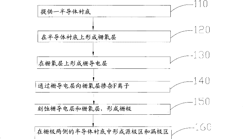
[0065] Please refer to figure 2 .
[0066] S110: Provide a semiconductor substrate.
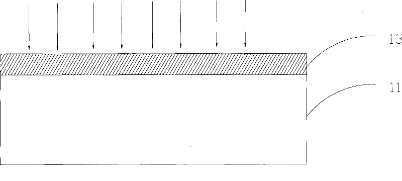
[0067] Such as image 3 As shown, a semiconductor substrate 100 is provided, and the semiconductor substrate 100 can be single crystal silicon, polycrystalline silicon or amorphous silicon; the semiconductor substrate 100 can also be silicon, germanium, gallium arsenide or silicon germanium compound; The semiconductor substrate 100 may also have an epitaxial layer or a silicon-on-insulator structure; the semiconductor substrate 100 may also be made of other semiconductor materials, which will not be listed here.
[0068] There may be a P well in the semiconductor substrate 100, and the P well may be formed by methods known to those skilled in the art, for example, on the semiconductor substrate 100, a region for forming the P well is first defined by a photolithography process , and then perform ion implantation to form a P well, and the implanted ions are P-type ions, such as boron ions....
Embodiment 2
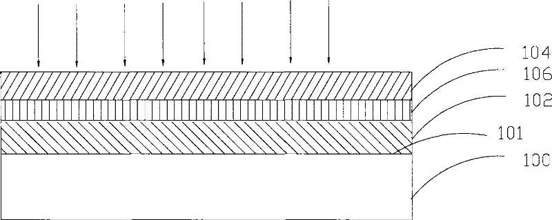
[0084] Please refer to Figure 3-Figure 5 .
[0085] S210: Provide a semiconductor substrate.
[0086] This step is the same as step S110 and will not be repeated here.
[0087] S220: forming a gate oxide layer on the semiconductor substrate.
[0088] This step is the same as step S120 and will not be repeated here.
[0089] S230: Doping F ions into the gate oxide layer 102 .
[0090] Therefore, in this embodiment, the gate oxide layer 102 is doped with F ions, so that the F ions enter the gate oxide layer 102 and generate Si-F bonds at the junction 101 between the gate oxide layer 102 and the semiconductor substrate 100, because The Si-F bond is very stable, so the interface state changes less when the temperature changes.
[0091] At the same time, because there is a nitrogen-containing thin layer 106 on the surface of the gate oxide layer 102 , this layer makes it difficult for boron ions to pass through when F ions enter the gate oxide layer 102 through the nitrogen-c...
Embodiment 3
[0100] Such as Figure 4 As shown, the present invention also provides a PMOS transistor, including a semiconductor substrate 100 with a gate on the semiconductor substrate 100, and the gate includes a gate oxide layer 102 and a gate conductor on the gate oxide layer 102. Layer 104 has a source region 110 and a drain region 112 in the semiconductor substrate 100 on both sides of the gate, and the interface 101 between the gate oxide layer 102 and the semiconductor substrate 100 has Si-F chemical bonds.
[0101] In addition, there may be a nitrogen-containing thin layer 106 at the interface of the gate oxide layer 102 in contact with the gate conductive layer 104 .
[0102] Because the Si-F bond is very stable, the interface state is stabilized, thereby increasing the NBTI. Moreover, because there is a nitrogen-containing thin layer 106 at the junction of the gate oxide layer 102 and the gate conductive layer 104, the penetration and diffusion of P-type ions are reduced, the g...
PUM
 Abstract
Description
Claims
Application Information