Method for manufacturing integrated micro four-point probe chip based on nano-processing technology

A four-point probe and nanofabrication technology, which is applied in the direction of nanotechnology, nanotechnology, nanostructure manufacturing, etc., can solve the problems of complex preparation process, fracture, inconsistent thermal expansion coefficient, etc., and achieve the effect of simple process method and improved yield

Inactive Publication Date: 2010-06-16
INST OF PHYSICS - CHINESE ACAD OF SCI
View PDF2 Cites 5 Cited by
  • Summary
  • Abstract
  • Description
  • Claims
  • Application Information

AI Technical Summary

Problems solved by technology

[0003] At present, in the method of making micro four-point probes, a silicon nitride film grown by low-pressure vapor deposition (LPCVD) is generally used as a protective mask (see Scanning microscopic four-point conductivity probes published by C.L.Petersen, T.M.Hansen et al., Sensors and actuators A96 (2002) 53-58), but because the silicon nitride itself is not dense enough, and the thermal expansion coefficient is inconsistent with silicon, not only cannot resist the long-term alkali corrosion process, but also easily causes the chip cantilever to bend and break ( See Figure 1), resulting in lower yield
It is also known to adopt a single silicon dioxide film or a chromium film as a mask (see Chinese patent application CN 101417890A "Silicon Nitride Wet Etching Method"), but because this mask is difficult to resist corrosion for a long time , it is easy to produce additional etching on the sample
At present, a method of using a composite film is also disclosed (see Chinese patent application CN101290362A "A Method for Making Multi-level Micro-mirrors by Wet Etching of Silicon"), but because of its complicated preparation process, it is not suitable for four-point micro-mirrors. Production of probes

Method used


Image

  • Method for manufacturing integrated micro four-point probe chip based on nano-processing technology
  • Method for manufacturing integrated micro four-point probe chip based on nano-processing technology
  • Method for manufacturing integrated micro four-point probe chip based on nano-processing technology

Examples


Embodiment Construction

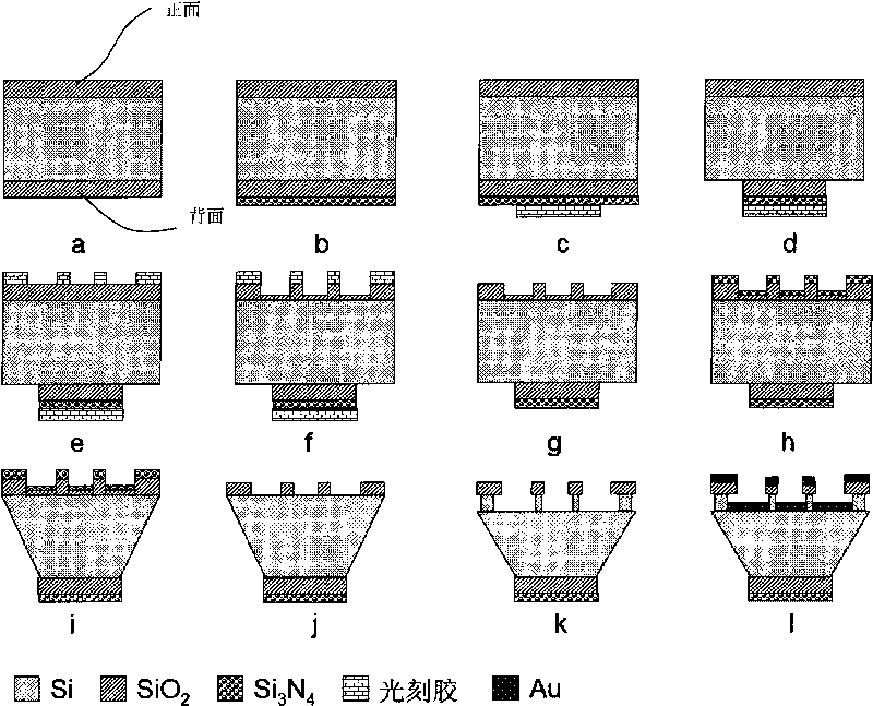
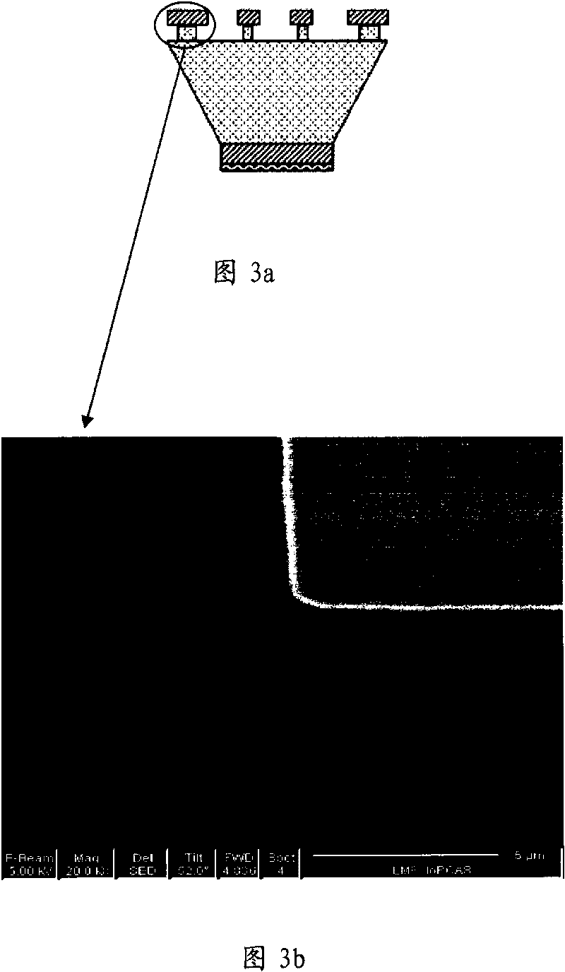
[0027] According to one embodiment of the present invention, there is provided an integrated micro four-point probe manufacturing method based on nanofabrication technology, the method comprising the following steps:

[0028] Step a): In the case of figure 2 (001) silicon wafer (crystal orientation / ) shown in a, silicon oxide layer (SiO 2 ) on one surface (i.e. the back) with a thickness of 1.3±0.3 microns), a layer of silicon nitride (Si 3 N 4 ) film (see figure 2 b), i.e. the first silicon nitride layer, the thickness of which is 50-500nm; then, a layer of S1813 positive photoresist is coated on the surface of the first silicon nitride by a centrifugal gluing machine, and the photoresist is exposed to ultraviolet light Exposure, fixation and development, thereby making the first photoresist mask on the silicon wafer backside (see figure 2 c); by reactive ion etching (RIE), remove the first silicon nitride layer and the first silicon oxide layer that are not protected by...


PUM

PropertyMeasurementUnit
thicknessaaaaaaaaaa
thicknessaaaaaaaaaa
thicknessaaaaaaaaaa

Abstract

The invention discloses a method for manufacturing an integrated micro four-point probe based on nano-processing technology, which comprises the following steps: a, growing a first silicon nitride layer on the back face of a double-face oxidized silicon slice and manufacturing a first photo-resist mask, and performing etching according to the mask pattern to expose silicon; b, manufacturing a second photo-resist mask on the front face of the silicon slice, removing the silicon oxide layer not covered by the second photo-resist mask on the front face of the silicon slice, but at least remaining a part, and growing a second silicon nitride layer on the front face after the removal of the photo-resist; and c, etching the sample obtained by the step b) in KOH solution, removing the second silicon nitride layer and the silicon oxide layer on the front face to expose the silicon, etching out an undercut structure, and finally growing a conductive layer on the front face. The manufacturing method has the advantage that: the thermal expansion coefficient of the mask is consistent with that of the silicon, the manufacturing process is simplified, and the yield is improved by remaining a silicon dioxide thin film on the surface of the silicon slice and then growing a silicon nitride thin film to realize a double-layer mask.

Description

technical field [0001] The invention belongs to the field of nano-processing, and more specifically relates to a method for manufacturing an integrated micro four-point probe chip based on nano-processing technology. Background technique [0002] Generally, the micro four-point probe is an electrical transport measurement device used on the crystal surface. Due to its fixed probe spacing and small mechanical constant of the probe, it can realize non-destructive measurement of surface resistance and ultra-thin sheet resistance at the micron scale. Measurement. [0003] At present, in the method of making micro four-point probes, a silicon nitride film grown by low-pressure vapor deposition (LPCVD) is generally used as a protective mask (see Scanning microscopic four-point conductivity probes published by C.L.Petersen, T.M.Hansen et al., Sensors and actuators A96 (2002) 53-58), but because the silicon nitride itself is not dense enough, and the thermal expansion coefficient i...

Claims


Application Information

Patent Timeline
Patent Type & Authority Applications(China)
IPC IPC(8): G01R27/02B82B3/00
Inventor 何杰辉吴克辉罗强顾长志郭建东
Owner INST OF PHYSICS - CHINESE ACAD OF SCI
Why Eureka
Try Eureka