
Organic semiconductor material and organic thin film transistor using the same

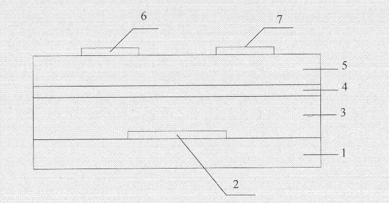
A thin-film transistor and organic semiconductor technology, applied in the field of organic thin-film transistors, can solve problems such as low electron mobility, achieve high-order thin films, facilitate efficient transmission, and improve electron mobility.

Inactive Publication Date: 2012-07-11
CHANGCHUN INST OF APPLIED CHEMISTRY - CHINESE ACAD OF SCI
View PDF0 Cites 0 Cited by
  • Summary
  • Abstract
  • Description
  • Claims
  • Application Information

AI Technical Summary

Problems solved by technology

[0005] However, the electron mobility of organic semiconductor materials in the prior art is low, which cannot meet the needs in practical applications.

Method used


Image

  • Organic semiconductor material and organic thin film transistor using the same
  • Organic semiconductor material and organic thin film transistor using the same
  • Organic semiconductor material and organic thin film transistor using the same

Examples


Embodiment 1

[0058] Into a 500 mL Schlenck reaction flask were added diethyl 2,5-dibromoterephthalate (5.60 g, 14.7 mmol), 5-hexyl-2-tributyltinylthiophene ( 15.5 g, 33.9 mmol), tetrakis (triphenylphosphine) palladium (330 mg, 0.285 mmol) and 250 ml of anhydrous N, N-dimethylformamide (abbreviated as DMF). Stir at 90° C. for 36 hours under dark conditions. Then the reaction mixture was cooled to room temperature, and 1 liter of water was added for liquid separation. The obtained aqueous layer was extracted three times with 50 ml of dichloromethane. The organic phases were combined, extracted twice with saturated brine, 100 ml each time, and dried with anhydrous magnesium sulfate. After the solvent was spin-dried, the reaction mixture was separated through a silica gel column, and the eluent was a mixed solvent of petroleum ether and dichloromethane (volume ratio of 2:1), and finally diethyl 2,5-bis[2'-( 7.42 g of 5'-dihexylthienyl)] terephthalate, and the yield was 91.0%. The reaction f...

Embodiment 2

[0063] Add diethyl 2,5-bis[2′-(5′-dihexylthienyl)]terephthalate (7.1 g , 12.8 mmol), potassium hydroxide (2.87 g, 51.2 mmol), 360 ml of ethanol and 47 ml of water, and the reaction mixture was heated to reflux overnight. After the reaction, the reaction solvent was concentrated to half under reduced pressure, 200 ml of water was added, and then hydrochloric acid with a concentration of 3 moles per liter was added dropwise until no precipitate was formed. The precipitate was filtered and vacuum-dried to obtain 6.21 g of 2,5-bis[2'-(5'-dihexylthienyl)]-1,4-terephthalic acid with a yield of 97.3%. The reaction formula is as follows:

[0064]

[0065] Wherein, R is a hexyl group.

[0066] H NMR spectrum characterization results: 1 H NMR (DMSO-d 6 , 300MHz): δ(ppm) 13.78(b, 2H), 7.05(d, J=3.6Hz, 2H), 6.85(d, J=3.6Hz, 2H), 2.81(t, J=7.5Hz, 4H) , 1.66-1.61 (m, 4H), 1.31-1.29 (m, 8H), 0.87 (t, J=6.6Hz, 6H).

Embodiment 3

[0068] Under an argon atmosphere, 2,5-bis[2′-(5′-dihexylthienyl)]terephthalic acid (4 g, 8.02 mg mol), oxalyl chloride (10.75 g, 84.7 mmol), 200 mL of anhydrous dichloromethane and 1 mL of anhydrous N,N-dimethylformamide. After the reaction mixture was stirred at room temperature for 12 hours, the solvent was distilled off under reduced pressure to obtain 2,5-bis[2'-(5'-dihexylthienyl)]terephthalic acid chloride. The reaction formula is as follows:

[0069]

[0070] Wherein, R is a hexyl group.


PUM

PropertyMeasurementUnit
thicknessaaaaaaaaaa
electron mobilityaaaaaaaaaa

Abstract

The embodiment of the invention discloses a compound. In the technical scheme, selecting a plane rigid trapezoid molecule s-indacene [1,2-b:5,6-b'] dithiophene containing sulphur atoms as a core, and utilizing the inter-lapping of pi electron cloud and the weak interaction of sulphur atoms to realize the strong interaction of the molecules; introducing dicyanovinyl of strong electron-withdrawing in the radial direction of the trapezoid core to reduce the unoccupied highest molecular orbital energy level of the molecule and simultaneously expand the degree of conjugation in the radial direction of the molecule so as to realize the effective injection and transmission of the electron; and introducing alkyl at the end of the trapezoid core to improve the self-organizing capability of the molecule during the process of film formation, thereby achieving a high ordered film to be used in an organic film transistor. The experiment shows that the electron mobility of the organic semiconductormaterial composed of the compound provided by the invention is 0.33cm2 / V.s, and the electron mobility of the organic semiconductor material provided by the invention is significantly increased than the electron mobility of the organic semiconductor material provided by the prior art.

Description

technical field [0001] The invention relates to the technical field of semiconductor materials, and more specifically, relates to an organic semiconductor material and an organic thin film transistor using the material. Background technique [0002] In recent years, the development of organic semiconductor materials with high carrier transport properties has been extremely active, showing broad application prospects in information display, integrated circuits, photovoltaic cells, and sensors. According to the difference of carrier types, organic semiconductor materials can be mainly divided into two categories: hole transport type and electron transport type, correspondingly called p-type organic semiconductor materials and n-type organic semiconductor materials. The synergistic development of hole-transporting and electron-transporting organic semiconductor materials with high mobility plays a crucial role in the development of p-n heterojunctions, bipolar field-effect tran...

Claims


Application Information

Patent Timeline
Patent Type & Authority Patents(China)
IPC IPC(8): C07D495/04H01L51/05H01L51/30
Inventor 耿延候田洪坤
Owner CHANGCHUN INST OF APPLIED CHEMISTRY - CHINESE ACAD OF SCI
Learn More