Production method for sapphire pattern substrate

A graphic substrate and manufacturing method technology, applied in semiconductor/solid-state device manufacturing, electrical components, circuits, etc., can solve the problems of low yield of LED chips, difficult control of the manufacturing process, and limitation of the internal quantum efficiency of light-emitting diodes, etc., to achieve The effect of reducing the cost of making PSS, the preparation method is simple and diverse, and the preparation process is easy to control

Inactive Publication Date: 2010-08-25
NANCHANG UNIV
View PDF7 Cites 19 Cited by
  • Summary
  • Abstract
  • Description
  • Claims
  • Application Information

AI Technical Summary

Problems solved by technology

[0002] Gallium nitride-based light-emitting diodes commonly used in the world are mainly heteroepitaxy on a flat substrate, where the substrate can be sapphire, silicon carbide or silicon. The main disadvantages of this structure are: 1. Since there is no lattice matching GaN-based light-emitting diodes are grown on substrates such as sapphire, silicon carbide, or silicon. The difference in lattice constants causes many dislocations in the epitaxial materials. These defects limit the light-emitting diodes. 2. When light enters the substrate from the epitaxial layer, because the interface is relatively flat, the incident angle of light is relatively small, and the refractive index difference between gallium nitride and the substrate is not large, resulting in low reflectivity, and most of the light will Escape to the substrate and cannot be effectively reflected back to the epitaxial layer, which greatly reduces the light extraction efficiency of GaN-based light-emitting diodes, especially the refractive index of the substrate of GaN-based blue-green light-emitting diodes with silicon carbide as the substrate. Gallium Nitride is comparable, 100% chance of light escaping from the epitaxial layer to the substrate
[0004] 1. Since the refractive index of sapphire is 1.8, which is relatively close to that of gallium nitride, when light enters the graphics substrate from the epitaxial layer, the reflectivity does not increase significantly, and the improvement of the light output rate of GaN-based light-emitting diodes is not as expected Effect
[0005] 2. Since the sapphire substrate is relatively hard, the production process has high requirements on equipment and technology, especially the dry etching of sapphire requires a helium cooling system and high-density plasma. Ordinary etching equipment cannot meet the requirements. Similarly, wet etching requires the use of strong acid at high temperature, and the production process is difficult to control, resulting in low yield and increased production costs.
However, sapphire is very hard. Dry etching (ICP etching) is required to etch micron-sized hills or other patterns, and it has high requirements for photolithography. It is necessary to use a photoresist with a thickness of more than 3 μm. Photoresist cylinders with a spacing of 1--3μm and a spacing of 0.5--2μm require advanced photolithography machines such as steppers, and it is difficult to ensure that there are no defects under a large-area sapphire substrate, so the cost of making PSS is very high. The excellent rate of LED chips is not high

Method used


Image

  • Production method for sapphire pattern substrate
  • Production method for sapphire pattern substrate
  • Production method for sapphire pattern substrate

Examples


Embodiment 1

[0029] A kind of manufacture method of sapphire pattern substrate, concrete steps are:

[0030] (1), on the upper surface of the 2-inch C-face sapphire substrate, utilize chemical vapor deposition to grow a layer of low-refractive index material, a film with a thickness of 500 angstroms, and the material of the film is silicon nitride (SiN);

[0031] (2), prepare hemispherical mask on silicon nitride film with photoresist;

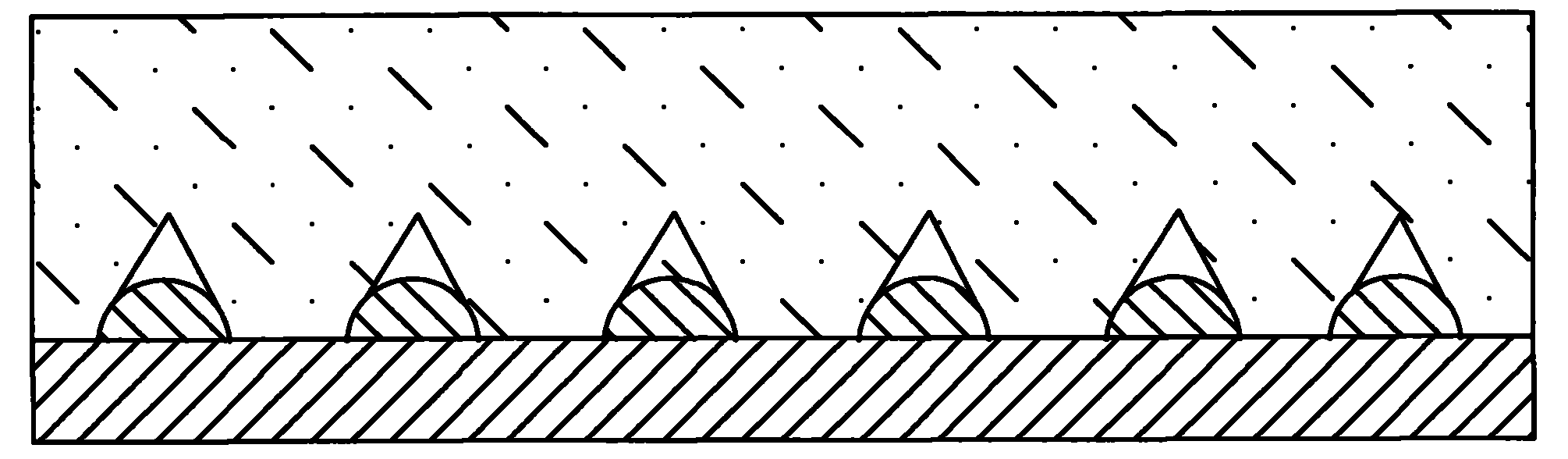
[0032] (3) By dry etching, the hemispherical photoresist mask pattern is transferred to the silicon nitride film, and hemispherical silicon nitride protrusions are formed on the sapphire substrate. The silicon nitride material between the hemispheres Etched clean to expose the sapphire substrate;

[0033] (4), with 150 degrees Celsius No. 3 solution (H 2 SO 4 :H 2 o 2 =3:1) to clean the sapphire substrate to prepare a sapphire pattern substrate.

[0034] The pattern of the gallium nitride-based light-emitting diode epitaxial substrate formed through ...

Embodiment 2

[0036] A kind of manufacture method of sapphire pattern substrate, concrete steps are:

[0037] (1), on the upper surface of the 2-inch sapphire substrate, utilize chemical vapor deposition to grow a layer of low-refractive index material, a film with a thickness of 400 angstroms, and the material of the film is silicon dioxide (SiO 2 );

[0038] (2), prepare conical mask on silicon dioxide thin film with photoresist;

[0039] (3) By dry etching, the conical photoresist mask pattern is transferred to the silicon dioxide film, and the conical silicon dioxide protrusions are formed on the sapphire substrate, and the silicon dioxide material between the cones Etched clean to expose the sapphire substrate;

[0040] (4), with 150 degrees Celsius No. 3 solution (H 2 SO 4 :H 2 o 2 =3:1) to clean the sapphire substrate to prepare a sapphire pattern substrate.

[0041] The pattern of the gallium nitride-based light-emitting diode epitaxial substrate formed through the above step...

Embodiment 3

[0043] A kind of manufacture method of sapphire pattern substrate, concrete steps are:

[0044] (1), on the upper surface of the 2-inch C-plane sapphire substrate, utilize chemical vapor deposition to grow a layer of low-refractive index material, a film with a thickness of 1 angstrom, and the material of the film is silicon nitride (SiN);

[0045] (2), prepare hemispherical mask on silicon nitride film with photoresist;

[0046] (3) By dry etching, the hemispherical photoresist mask pattern is transferred to the silicon nitride film, and hemispherical silicon nitride protrusions are formed on the sapphire substrate. The silicon nitride material between the hemispheres Etched clean to expose the sapphire substrate;

[0047] (4), with 150 degrees Celsius No. 3 solution (H 2 SO 4 :H 2 o 2 =3:1) to clean the sapphire substrate to prepare a sapphire pattern substrate.

[0048] The pattern of the gallium nitride-based light-emitting diode epitaxial substrate formed through th...


PUM

PropertyMeasurementUnit
widthaaaaaaaaaa
heightaaaaaaaaaa
thicknessaaaaaaaaaa

Abstract

The invention discloses a production method for a sapphire pattern substrate, comprising the following particular steps of (1) depositing a layer of thin film on the upper surface of a sapphire which has a low refractive index material and 1AA-999AA thickness; (2) preparing a mask pattern on the thin film with photoresistance; (3) transferring the pattern masked with photoresist to the thin film through etching to obtain a protuberance with the 1AA-999AA thickness, wherein the lower substrate of the pattern of the protuberance has a width of 0.5-3 mu m and a gap of 0.5-3 mu m; and (4) cleaning the sapphire to remove the residual photoresistance. The invention has the advantages that PSS cost can be greatly reduced and total reflection angles are increased for light, thereby being more favorable for emergent light, improving emergent light efficiency, being favor of laser peeling and increasing excellent rate of the finished product LED chip.

Description

technical field [0001] The invention relates to semiconductor materials, in particular to a manufacturing method of a sapphire pattern substrate. Background technique: [0002] Gallium nitride-based light-emitting diodes commonly used in the world are mainly heteroepitaxy on a flat substrate, where the substrate can be sapphire, silicon carbide or silicon. The main disadvantages of this structure are: 1. Since there is no lattice matching GaN-based light-emitting diodes are grown on substrates such as sapphire, silicon carbide, or silicon. The difference in lattice constants causes many dislocations in the epitaxial materials. These defects limit the light-emitting diodes. 2. When light enters the substrate from the epitaxial layer, because the interface is relatively flat, the incident angle of light is relatively small, and the refractive index difference between gallium nitride and the substrate is not large, resulting in low reflectivity, and most of the light will Esca...

Claims


Application Information

Patent Timeline
Patent Type & Authority Applications(China)
IPC IPC(8): H01L21/00
Inventor 江风益
Owner NANCHANG UNIV
Why Eureka
Try Eureka