Manufacturing method for monolithic integrated device of electrical absorption modulator and self-pulsation laser

An electro-absorption modulator and integrated device technology, which is applied to laser components, lasers, laser devices, etc., can solve the problems of large power loss, high cost, and large system volume, so as to reduce power loss and production costs and improve stability. sexual effect

Active Publication Date: 2010-09-08
INST OF SEMICONDUCTORS - CHINESE ACAD OF SCI
View PDF0 Cites 15 Cited by
  • Summary
  • Abstract
  • Description
  • Claims
  • Application Information

AI Technical Summary

Problems solved by technology

[0005] At present, the direct modulation loading of self-pulsating laser data mainly uses discrete Mach-Zehnder (MZM

Method used


Image

  • Manufacturing method for monolithic integrated device of electrical absorption modulator and self-pulsation laser
  • Manufacturing method for monolithic integrated device of electrical absorption modulator and self-pulsation laser
  • Manufacturing method for monolithic integrated device of electrical absorption modulator and self-pulsation laser

Examples


Embodiment Construction

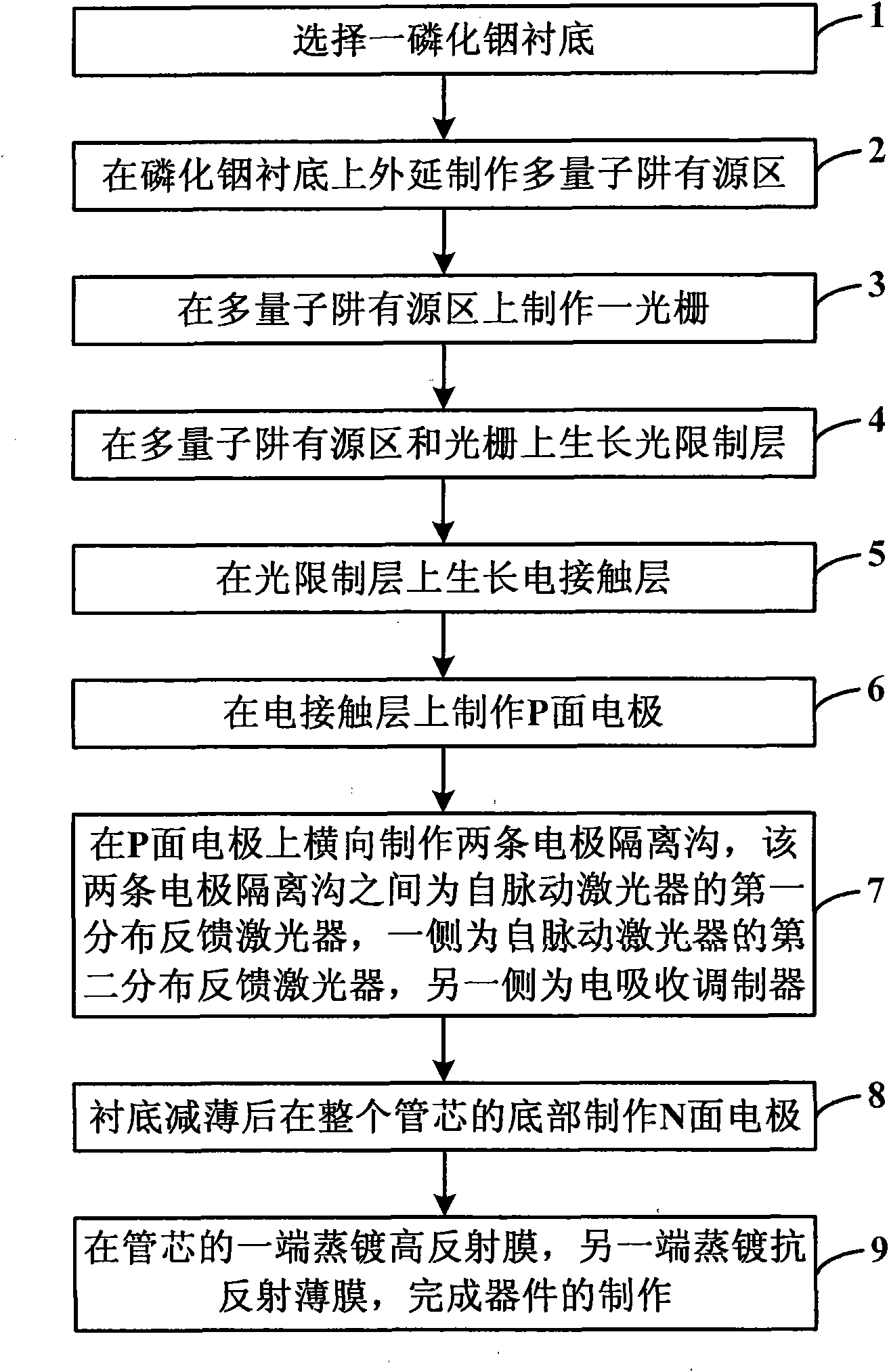
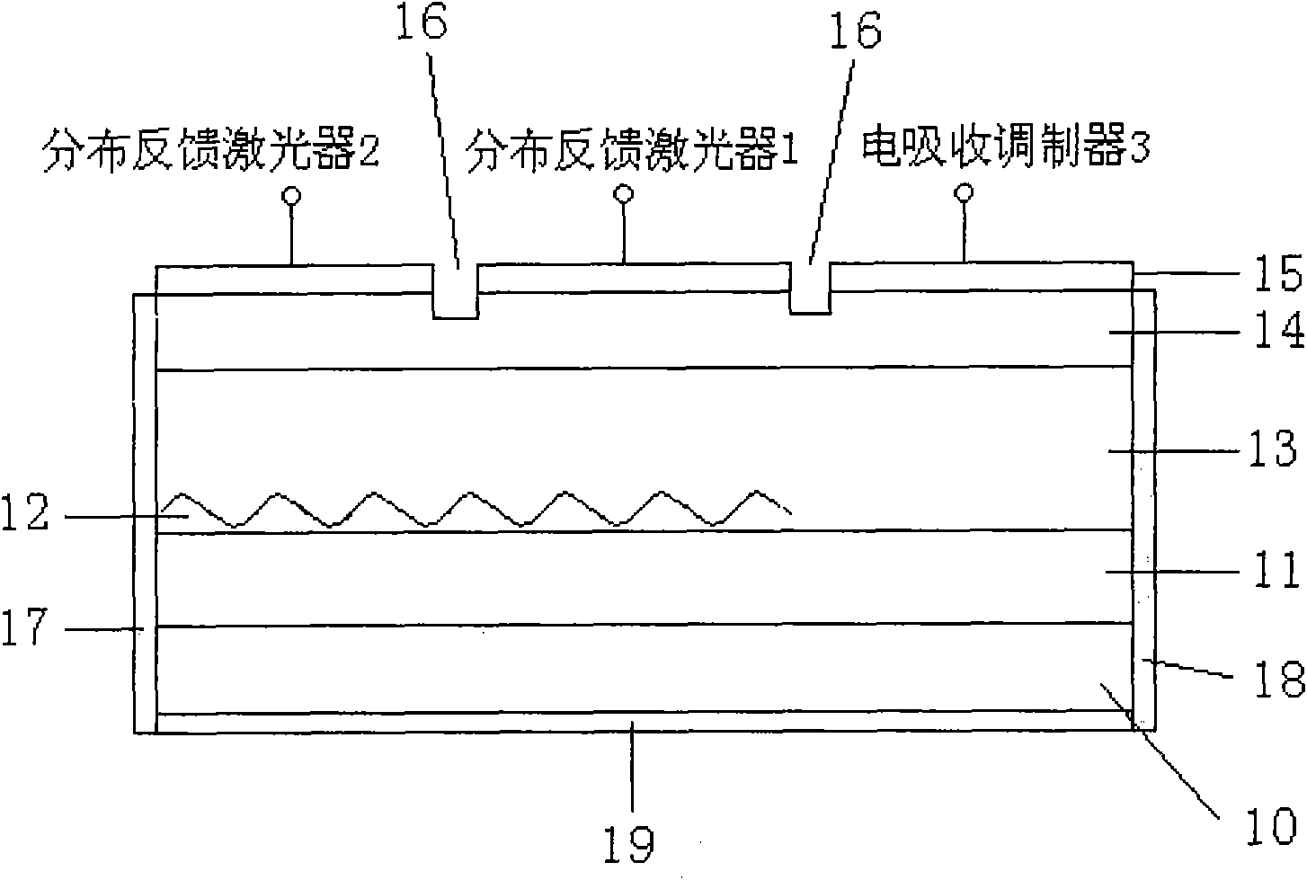
[0033] In order to make the object, technical solution and advantages of the present invention clearer, the present invention will be described in further detail below in conjunction with specific embodiments and with reference to the accompanying drawings.

[0034] Please refer to figure 1 and figure 2 , figure 2 It is a structural schematic diagram of an electroabsorption modulator and a self-pulsation laser monolithic integrated device produced by the present invention, figure 1 It is a flowchart of a method for manufacturing an electroabsorption modulator and a self-pulsation laser monolithic integrated device provided by the present invention, and the method includes the following manufacturing steps:

[0035] 1), select an indium phosphide substrate 10;

[0036] 2) On the indium phosphide substrate 10, the multi-quantum well active region 11 is made epitaxially, which is made of indium gallium arsenic phosphorus material, and the thickness is 70 to 120 nanometers. I...


PUM

PropertyMeasurementUnit
Thicknessaaaaaaaaaa

Abstract

The invention discloses a manufacturing method for a monolithic integrated device of an electrical absorption modulator and a self-pulsation laser, which comprises the steps of: selecting an indium phosphide substrate; manufacturing a multiple-quantum-well active region on the extension of the indium phosphide substrate; manufacturing a grating on the multiple-quantum-well active region; growing optical limiting layers on the multiple-quantum-well active region and the grating; growing electrical contact layers on the optical limiting layers; manufacturing P-surface electrodes on the electrical contact layers; transversely manufacturing two electrode isolating channels on the P-surface electrodes; installing a first distributing feedback laser of the self-pulsation laser between the two electrode isolating channels; installing a second distributing feedback laser of the self-pulsation laser on one side; installing the electrical absorption modulator on the other side; thinning the substrate; manufacturing N-surface electrodes on the bottom of a whole pipe core; evaporating and plating a high-reflection film on one end of the pipe core; and evaporating and plating an anti-reflection film on the other end to finish the manufacture of the device. The invention reduces the power loss and the manufacturing cost of a ROF (Rate Of Fire) system emitter, and enhances system stability.

Description

technical field [0001] The invention relates to the field of optoelectronic devices, in particular to a method for manufacturing an electroabsorption modulator and a self-pulsation laser monolithic integrated device. Background technique [0002] The basic components of a multi-segment self-pulsating laser are two distributed feedback lasers, which are tuned by current or using gratings with different Bragg wavelengths. The emission wavelengths of the two lasers have a shift of about several nanometers. When the laser light emitted by the self-pulsation laser is irradiated on the detector, a self-pulsation signal with a frequency equal to the difference between the emission frequencies of the two distributed feedback lasers will be generated. [0003] Compared with other forms of laser-based microwave sources, multi-segment self-pulsating lasers have the advantage of compact structure, and their self-pulsation frequency can be flexibly adjusted in a wide range by injection c...

Claims


Application Information

Patent Timeline
IPC IPC(8): H01S5/026H01S5/40H01S5/12H01S5/343G02F1/017
Inventor 梁松孔端花朱洪亮王圩
Owner INST OF SEMICONDUCTORS - CHINESE ACAD OF SCI
Why Eureka
Try Eureka