Method for growing semi-polar GaN based on Al2O3 substrate with m sides

A semi-polar, substrate technology, applied in the field of microelectronics, can solve the problems of increasing process flow and low efficiency, and achieve the effect of improving luminous efficiency, high efficiency, and reducing the influence of mechanical stress

Active Publication Date: 2010-09-29
云南凝慧电子科技有限公司
View PDF4 Cites 19 Cited by
  • Summary
  • Abstract
  • Description
  • Claims
  • Application Information

AI Technical Summary

Problems solved by technology

However, in this SLEO method, after the GaN substrate is grown, SiO 2 The process of deposition and photolithography greatly increases the process flow, and the efficiency is low

Method used


Image

  • Method for growing semi-polar GaN based on Al2O3 substrate with m sides
  • Method for growing semi-polar GaN based on Al2O3 substrate with m sides
  • Method for growing semi-polar GaN based on Al2O3 substrate with m sides

Examples


Embodiment 1

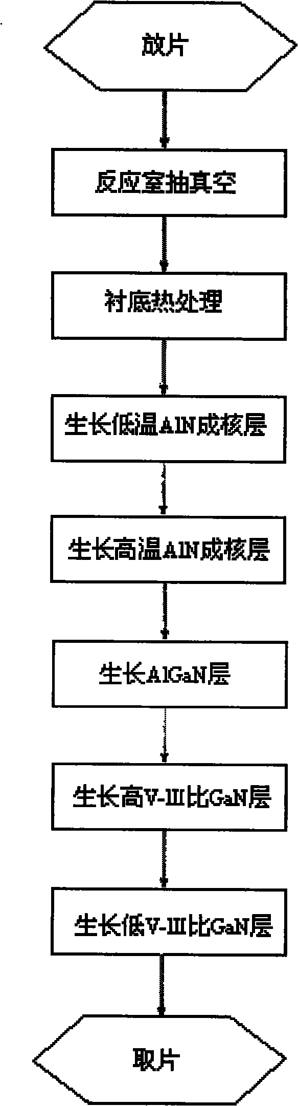
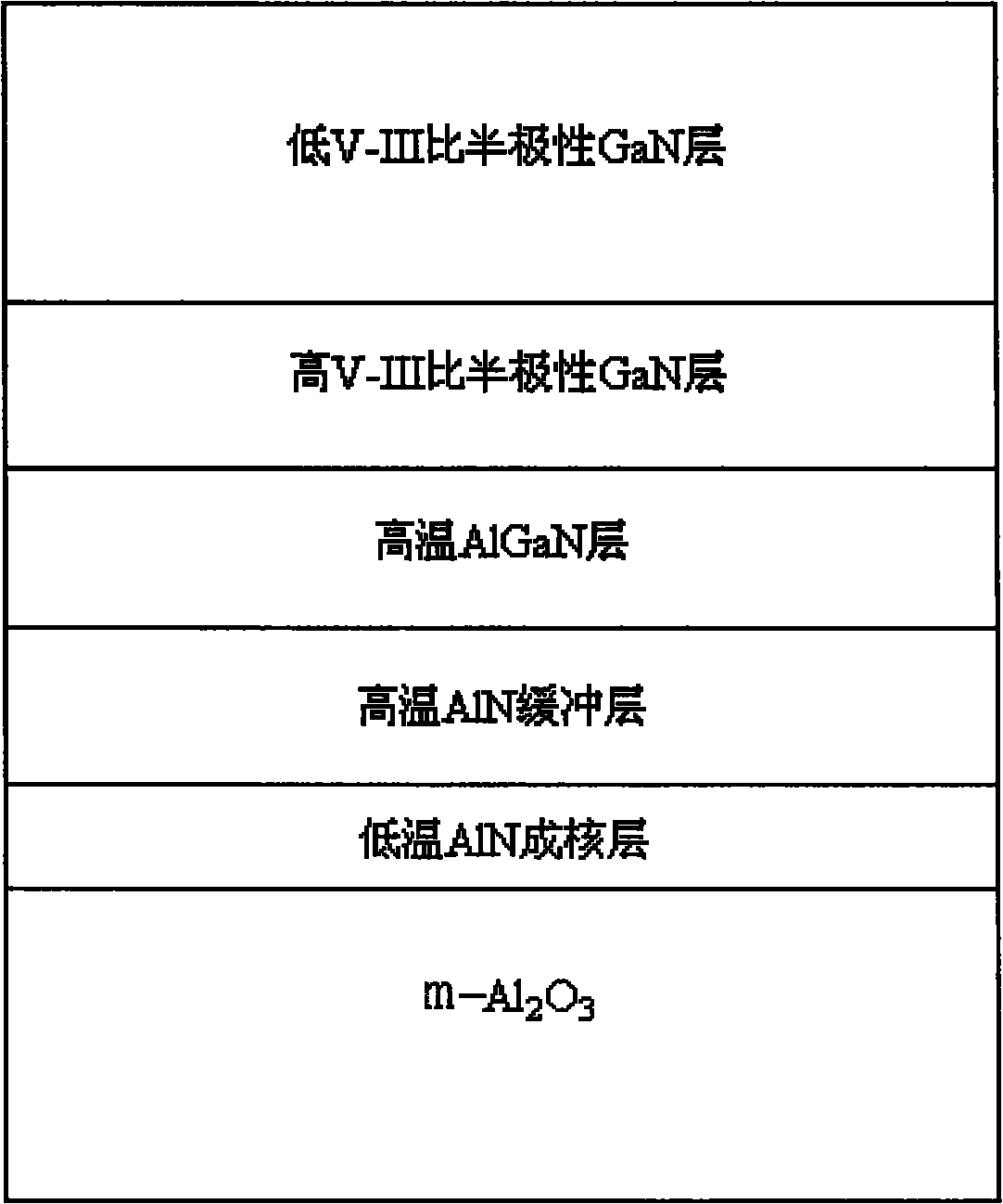
[0023] Step 1, performing heat treatment on the substrate substrate.

[0024] Al 2 o 3 The substrate is placed in the metal organic compound chemical vapor deposition MOCVD reaction chamber, and the mixed gas of hydrogen and ammonia is introduced into the reaction chamber, and the vacuum degree in the reaction chamber is less than 2×10 -2 Torr, under the condition that the substrate heating temperature is 1100° C., the time is 8 minutes, and the pressure of the reaction chamber is 40 Torr, heat treatment is performed on the substrate.

[0025] Step 2, growing a low-temperature AlN layer.

[0026] Lower the temperature of the heat-treated substrate to 620°C, feed the aluminum source with a flow rate of 15 μmol / min, hydrogen gas with a flow rate of 1200 sccm and ammonia gas with a flow rate of 1500 sccm into the reaction chamber, and grow the thickness under the condition of maintaining a pressure of 40 Torr A low temperature AlN nucleation layer of 20nm.

[0027] Step 3, gr...

Embodiment 2

[0037] Step A, performing heat treatment on the base substrate.

[0038] Al 2 o 3 The substrate is placed in the metal organic compound chemical vapor deposition MOCVD reaction chamber, and the mixed gas of hydrogen and ammonia is introduced into the reaction chamber, and the vacuum degree in the reaction chamber is less than 2×10 -2 Torr, under the condition that the substrate heating temperature is 900° C., the time is 5 minutes, and the pressure of the reaction chamber is 20 Torr, heat treatment is performed on the substrate.

[0039] Step B, growing a low-temperature AlN layer.

[0040] Lower the temperature of the heat-treated substrate to 500°C, feed the aluminum source with a flow rate of 5 μmol / min, hydrogen gas with a flow rate of 1200 sccm, and ammonia gas with a flow rate of 1000 sccm into the reaction chamber, and grow thickness under the condition of maintaining a pressure of 20 Torr A low temperature AlN nucleation layer of 20nm.

[0041]Step C, growing a hig...

Embodiment 3

[0051] Step I, heat-treating the base substrate.

[0052] Al 2 o 3 The substrate is placed in the metal organic compound chemical vapor deposition MOCVD reaction chamber, and the mixed gas of hydrogen and ammonia is introduced into the reaction chamber, and the vacuum degree in the reaction chamber is less than 2×10 -2 Torr, under the condition that the substrate heating temperature is 1200° C., the time is 10 min, and the pressure of the reaction chamber is 760 Torr, heat treatment is performed on the substrate.

[0053] Step II, growing a low-temperature AlN layer.

[0054] Lower the temperature of the heat-treated substrate to 650°C, feed the aluminum source with a flow rate of 100 μmol / min, hydrogen gas with a flow rate of 1200 sccm, and ammonia gas with a flow rate of 10000 sccm into the reaction chamber, and grow the thickness under the condition of maintaining a pressure of 760 Torr A low temperature AlN nucleation layer of 200nm.

[0055] Step III, growing a high t...


PUM

PropertyMeasurementUnit
thicknessaaaaaaaaaa
thicknessaaaaaaaaaa
thicknessaaaaaaaaaa

Abstract

The invention discloses a method for growing a semi-polar GaN membrane based on an Al2O3 substrate with m sides and mainly solves the problems that the conventional semi-polar material has poorer quality and non-attractive surface appearance. The method comprises the following steps of: (1) arranging an Al2O3 substrate with m sides in to an MOCVD (Metal Organic Chemical Vapor Deposition) reaction chamber, introducing the mixed gas of hydrogen and ammonia to the reaction chamber, and thermally processing the substrate; (2) growing a low-temperature AlN (Aluminium Nitride) layer with thickness of 20 to 200 nm and temperature of 500 to 650 DEG C on the Al2O3 substrate with m sides; (3) growing a high-temperature AlN layer with thickness of 50 to 200 nm and temperature of 1000 to 1150 DEG C on the low-temperature AlN layer; (4) growing a high-temperature AlGaN layer with thickness of 50 to 500 nm and temperature of 1000 to 1150 DEG C on the high-temperature AlN layer; (5) growing a semi-polar GaN layer with high V-III ratio, the thickness of 50 to 1000 nm and the temperature of 1000 to 1150 DEG C on the high-temperature GaN layer; and (6) growing a semi-polar GaN layer with low V-III ratio, the thickness of 1000 to 10000 nm and the temperature of 1000 to 1150 DEG C on the semi-polar GaN layer with high V-III ratio. The invention has the advantages of simple process and little fault, and is applied to manufacturing the semi-polar GaN light-emitting diodes and the lasers.

Description

technical field [0001] The invention belongs to the technical field of microelectronics, and relates to a method for growing semiconductor materials, in particular to an m-plane Al 2 o 3 The epitaxial growth method of a semipolar GaN semiconductor material on a substrate can be used to manufacture a semipolar GaN-based semiconductor device. technical background [0002] Gallium nitride and III-V nitrides have made great progress in the fields of optoelectronics and microelectronics. This material can work at high temperature and in relatively harsh environments, and has broad application prospects. It is currently a research hotspot. Conventional gallium nitride is grown on the polar c-plane. The excellent performance of GaN-based devices is mainly due to the existence of high-density and high-mobility two-dimensional electron gas (2DEG) at the AlGaN / GaN heterojunction interface. The 2DEG results from the large conduction band discontinuity in the heterojunction and the st...

Claims


Application Information

Patent Timeline
Patent Type & Authority Applications(China)
IPC IPC(8): H01L21/205C23C16/44
Inventor 郝跃许晟瑞周小伟张进成
Owner 云南凝慧电子科技有限公司
Why Eureka
Try Eureka