
Eureka
For R&D, Eureka makes reading and utilizing patents & technical documents easy.
Eureka AIR
Designed for self-driven R&D workflows. Generate viable solutions, solve complex R&D challenges, empower your innovation with AI.

Eureka Materials
Designed for material experts only. Revolutionize your material R&D, from search, analyze, to developing new materials.

TechResearch
Generate reliable direction feasibility study reports for your R&D in just a few steps.

TechSeek
Discover and master advanced knowledge NOW. Basics, ideas, possibilities, all at once.

TechMind
As an expert in R&D Theories, TechMind can generates customized viable solutions instantly.

TechRisk
Analyze your overall solution with one click, know your potential R&D risks in advance.

TechMonitor
Get weekly tech updates, stay abreast of the latest tech innovations and key insights.
Silicon-based multijunction multi-laminated PIN thin film solar cell with high conversion rate and production method thereof
A solar cell and high conversion rate technology, applied in the field of solar cells, can solve the problems of low solar conversion efficiency and silicon-based thin-film solar cell conversion rate to be improved, achieve high photoelectric conversion efficiency, increase light absorption efficiency, and improve conversion efficiency Effect
- Summary
- Abstract
- Description
- Claims
- Application Information
AI Technical Summary
Problems solved by technology
Method used
Image

Examples
Embodiment 1
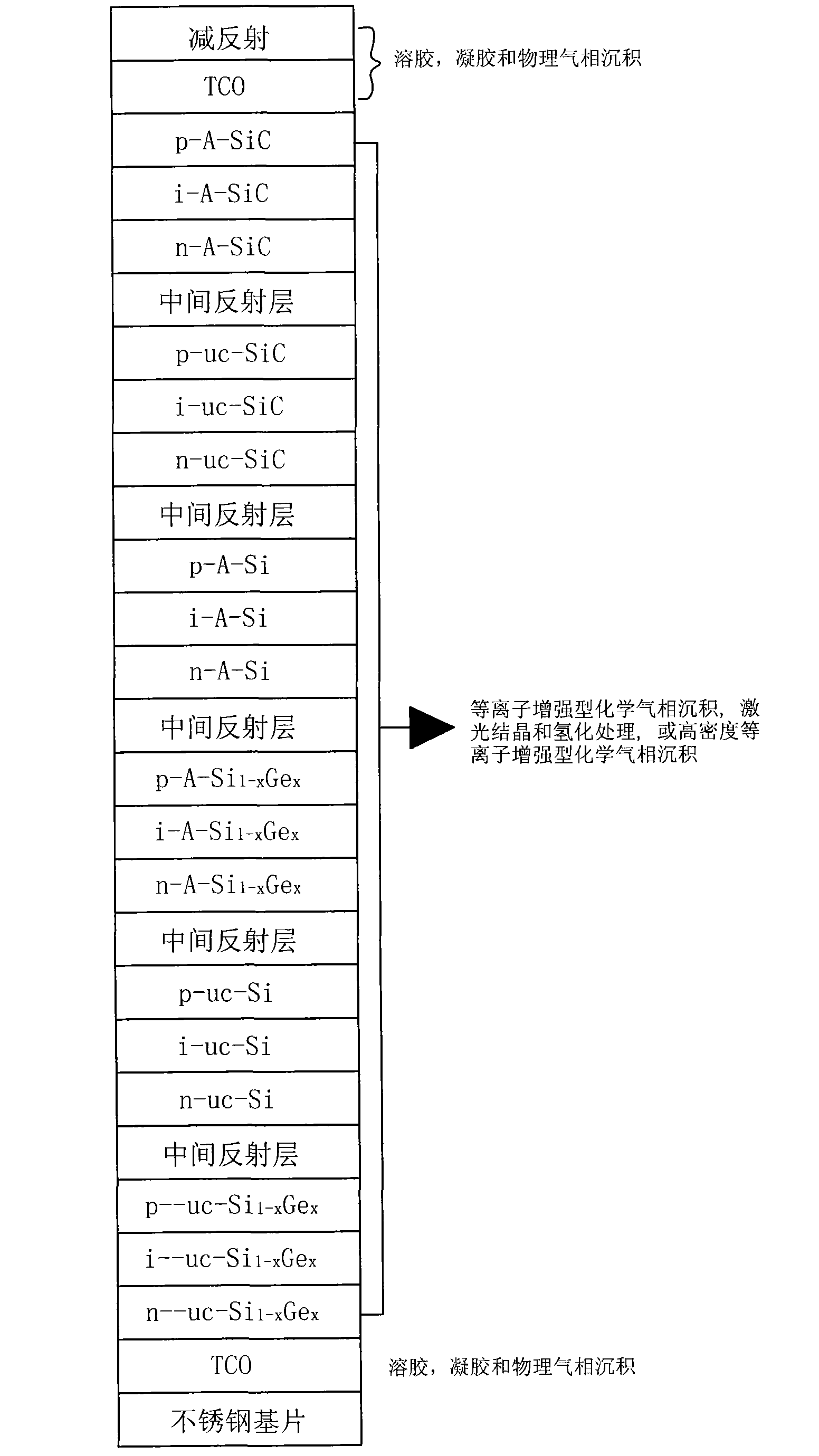
[0063] Example 1: Thin-film solar cell with multi-junction and multi-stack structure based on stainless steel
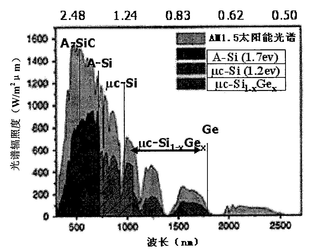
[0064] (1) Battery structure: stainless steel / TCO / n-μc-Si 1-x Ge x / i-μc-Si 1-x Ge x / p-μc-Si 1-x Ge x / intermediate reflective layer / n-μc-Si / i-μc-Si / p-μc-Si / intermediate reflective layer / n-A-Si 1-x Ge x / i-A-Si 1- x Ge x / p-A-Si 1-x Ge x / intermediate reflective layer / n-A-Si / i-A-Si / p-A-Si / intermediate reflective layer / n-μc-SiC / i-μc-SiC / p-μc-SiC / intermediate reflective layer / n-A-SiC / i-A-SiC / p-A-SiC / TCO / anti-reflection coating;
[0065] (2) Preparation process:
[0066] 1. After cleaning the stainless steel sheet, use PVD method to prepare ZnO:Ag, Al thin film (or use sol-gel method), then dry it, and then heat treatment at 400 ° C for 1 minute to 10 minutes in a hydrogen-containing atmosphere;
[0067] 2. Deposition of phosphorus (P) doped amorphous A-Si by PECVD method 1-x Ge x Thin film (1>x>0 uniform transition), then laser crystallization to form...
Embodiment 2
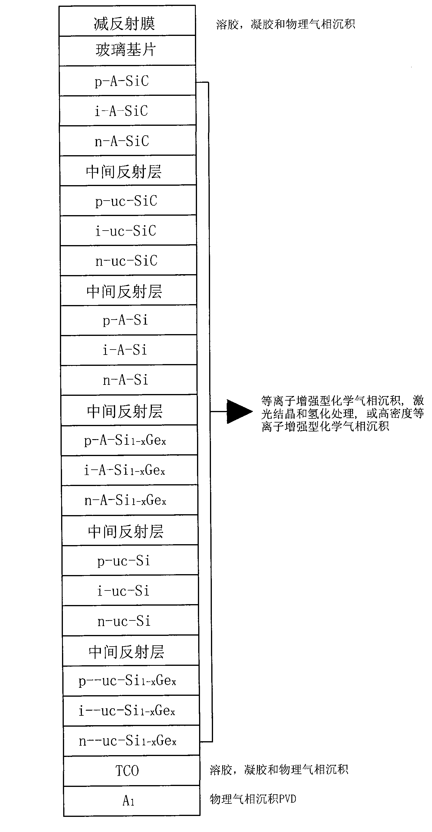
[0087] Example 2: Thin-film solar cell with glass substrate multi-junction multi-layer structure
[0088] (1) Battery structure: anti-reflection film / glass / TCO / p-A-SiC / i-A-SiC / n-A-SiC / intermediate reflection layer / p-μc-SiC / i-μc-SiC / n-μc-SiC / intermediate reflection layer / p-A-Si / i-A-Si / n-A-Si / intermediate reflection layer / p-A-Si 1-x Ge x / i-A-Si 1-x Ge x / n-A-Si 1-x Ge x / intermediate reflective layer / p-μc-Si / i-μc-Si / n-μc-Si / intermediate reflective layer / p-μc-Si 1-x Ge x / i-μc-Si 1-x Ge x / n-μc-Si 1- x Ge x / TCO / Al;
[0089] (2) The preparation process is as follows:
[0090] 1. After cleaning the glass sheet, use PVD method to prepare ZnO:Ag, Al thin film (or prepare it by sol-gel method), then dry it, and then heat treat it at 400°C for 1 minute to 10 minutes in a hydrogen-containing atmosphere;
[0091] 2. Deposit p-type boron (B)-doped amorphous A-SiC, i-type amorphous A-SiC, phosphorus (P)-doped n-type amorphous A-SiC films by PECVD method or HD-PECVD method , ...
PUM
| Property | Measurement | Unit |
|---|---|---|
| Aperture | aaaaa | aaaaa |
| Thickness | aaaaa | aaaaa |
| Thickness | aaaaa | aaaaa |
Abstract
Description
Claims
Application Information
 - R&D Engineer
- R&D Manager
- IP Professional
- Industry Leading Data Capabilities
- Powerful AI technology
- Patent DNA Extraction
Browse by: Latest US Patents, China's latest patents, Technical Efficacy Thesaurus, Application Domain, Technology Topic, Popular Technical Reports.
© 2024 PatSnap. All rights reserved.Legal|Privacy policy|Modern Slavery Act Transparency Statement|Sitemap|About US| Contact US: help@patsnap.com