Method for preparing patterned graphene

A patterned graphene and graphene technology, which is applied in the photoplate making process of the patterned surface, optical mechanical equipment, instruments, etc., can solve the problems of high cost and complex template manufacturing process, and achieve low cost and low device performance. Effect

Inactive Publication Date: 2010-10-27
PEKING UNIV
View PDF4 Cites 56 Cited by
  • Summary
  • Abstract
  • Description
  • Claims
  • Application Information

AI Technical Summary

Problems solved by technology

This method requires different templates for graphene with different graphics,

Method used


Image

  • Method for preparing patterned graphene
  • Method for preparing patterned graphene
  • Method for preparing patterned graphene

Examples


Embodiment Construction

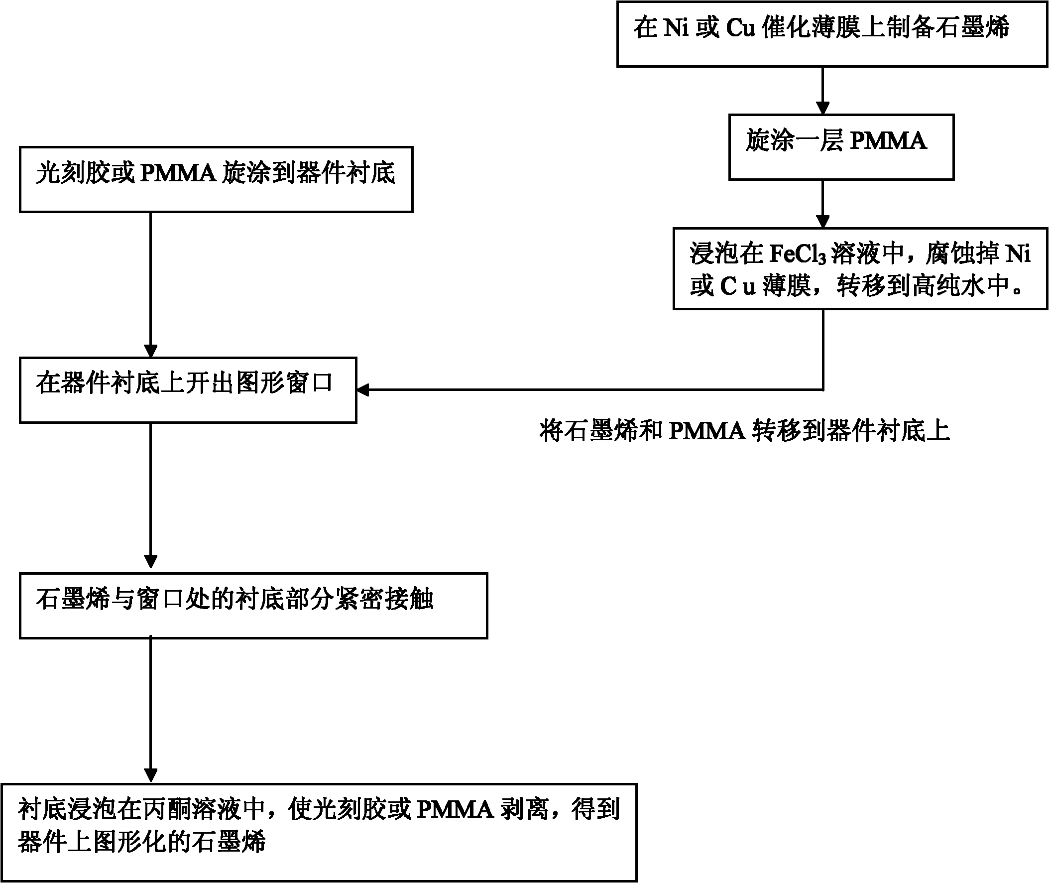
[0020] The invention adopts traditional micro-processing techniques such as photolithography, heat treatment, and stripping, and combines the conventional method of graphene transfer to prepare patterned graphene at the required place of the device substrate. This new etching-free graphene patterning method has broad application prospects in new devices with graphene as the functional unit. The main experimental process is as figure 1 As shown, the steps are as follows:

[0021] 1. Prepare large-area high-quality graphene on Ni or Cu catalytic film by chemical vapor deposition.

[0022] 2. Spin-coat a layer of PMMA on the graphene-grown substrate, for example: 2000rpm, 2 minutes.

[0023] 3. Soak the substrate with PMMA and graphene in 1M FeCl 3 solution, eg: 6 hours. The Ni layer is etched away, leaving the graphene and PMMA layers floating in the solution.

[0024] 4. Spin-coat photoresist (or PMMA) onto the target device substrate.

[0025] 5. Through ultraviolet lith...


PUM


Abstract

The invention discloses a method for preparing patterned graphene. In the method, a photoresist is patterned on a device substrate by a microelectronic process such as UV lithography and electron beam lithography, and windows are formed at positions needing graphene; by a graphene transfer method, large-area graphene is transferred onto the patterned photoresist; and the photoresist and the graphene thereon are stripped by an acetone immersion method so as to obtain the patterned graphene required by the device. Compared with the prior art, the method has the advantages of accurate positioning, and does not require etching or manufacturing an imprint template so as to have low cost. Through the method, the patterned graphene is accurately positioned, and the integration of large-area devices is easy to realize. Besides, by exposure and stripping methods, an oxygen plasma-etching step is avoided, so the reduction of the device performance caused by radiation damage is avoided.

Description

technical field [0001] The invention belongs to the technical field of graphene device preparation, and in particular relates to a method for preparing precisely positioned patterned graphene. Background technique [0002] Graphene is a two-dimensional crystal composed of carbon atoms in a honeycomb arrangement. Due to its quantum transport properties, high conductivity, mobility, and transmittance, graphene and its related devices have become a research hotspot in the fields of physics, chemistry, biology, and material science. So far, people have prepared a variety of devices with graphene as the basic functional unit, including field effect transistors, solar cells, nanogenerators, sensors, etc. Recently, large-area high-quality graphene has been successfully prepared by chemical vapor deposition on Ni or Cu catalytic films, which has promoted the application of graphene in devices. [0003] Graphene-based micro-nano electronic devices usually require precise positionin...

Claims


Application Information

Patent Timeline
IPC IPC(8): G03F7/00
Inventor 叶堉戴伦代宇秦国刚
Owner PEKING UNIV
Why Eureka
Try Eureka