Carbon-based nano novel field electron emission material in areatus layered structure and preparation method thereof

A technology of field electron emission and carbon-based nanomaterials, which is applied in the direction of nanostructure manufacturing, nanotechnology, nanotechnology, etc., can solve the problems of poor reliability and emission efficiency of a single carbon nanotube, and achieve the limitation of expanding applications , Improve the viscosity coefficient, improve the effect of mechanical properties

Active Publication Date: 2010-11-17
CHONGQING XINHE QIYUE TECH CO LTD
View PDF2 Cites 5 Cited by
  • Summary
  • Abstract
  • Description
  • Claims
  • Application Information

AI Technical Summary

Problems solved by technology

[0013] In addition, the second object of the present invention is to provide a method for preparing a carbon-based nano-type new field electron emission material with a clustered layered structure, which is aimed at the poor reliability of a single carbon nanotube and the easy degradation of carbon nanotubes under high voltage. However, the disadvantages such as the decrease of emission efficiency are caused, and the combination of carbon nanomaterials and substrates is strengthened by a new method to enhance its own strength and reliability; at the same time, the surface area of ​​carbon-based materials is increased, and the density of electron emission sources is increased.

Method used


Image

  • Carbon-based nano novel field electron emission material in areatus layered structure and preparation method thereof
  • Carbon-based nano novel field electron emission material in areatus layered structure and preparation method thereof
  • Carbon-based nano novel field electron emission material in areatus layered structure and preparation method thereof

Examples


Embodiment 1

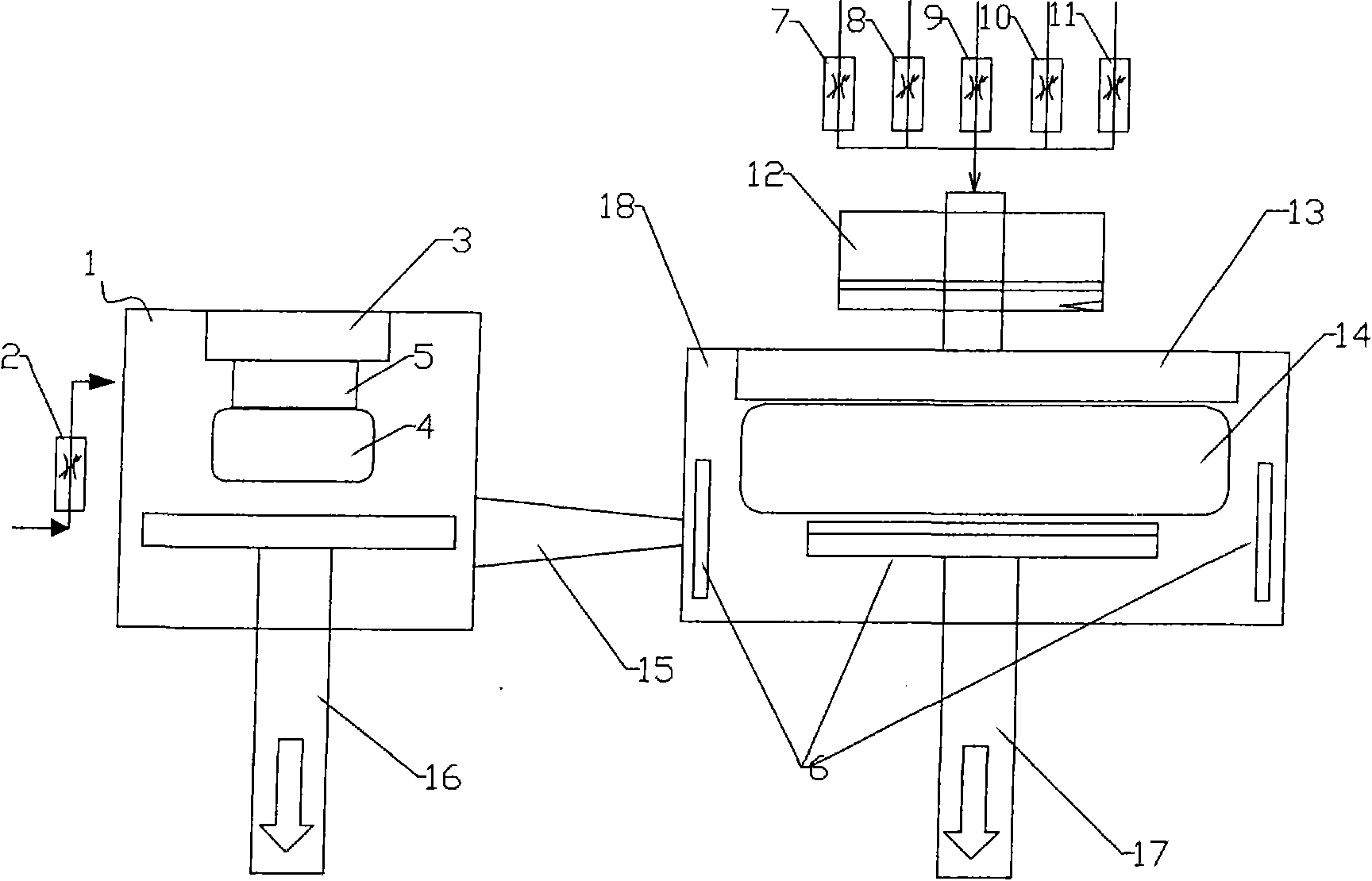
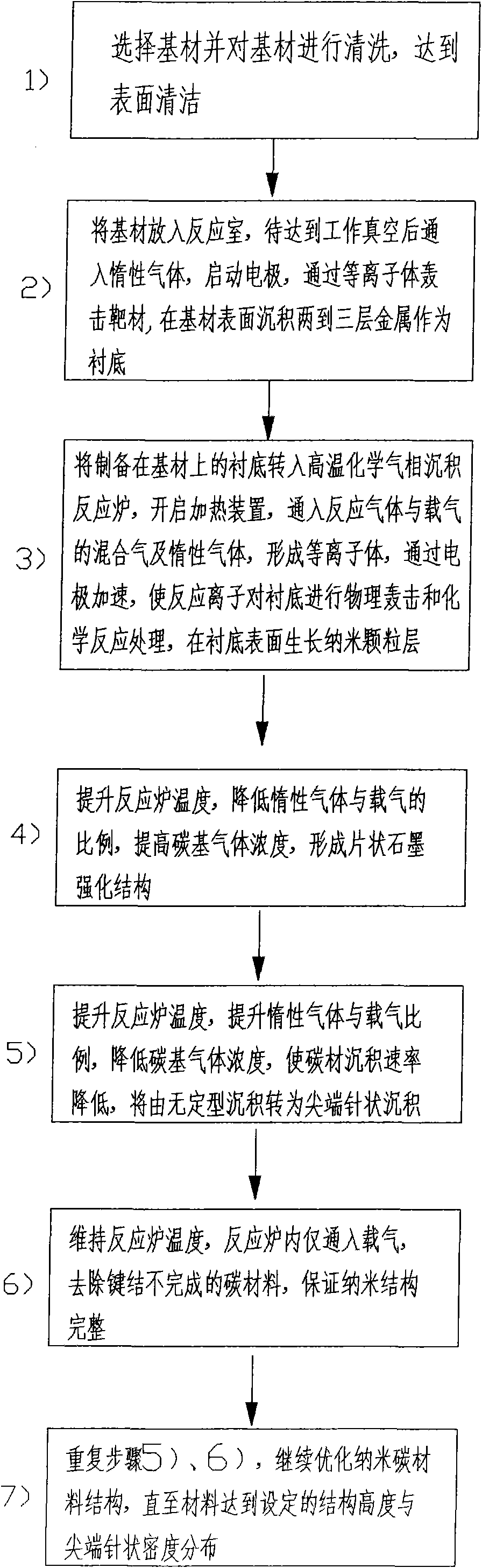
[0052] Such as figure 1 and figure 2 Shown, method of the present invention comprises the following steps:

[0053] 1) Select a metal (such as copper) suitable for the growth of carbon nanomaterials as the substrate, and perform physical and chemical cleaning on the substrate to achieve the surface cleanliness required for deposition;

[0054] 2) Load the cleaned substrate into the magnetron sputtering reaction chamber 1, start the vacuum units 16 and 17, and wait until the vacuum degree reaches 8×10 -4 At Pa, the inert gas is introduced through the flow meter 2 to raise the vacuum degree to 1 Pa and keep it stable, the electrode 3 is started to form a plasma 4, and the target material 5 is bombarded by the plasma to deposit different two to three layers on the substrate. Metal is used as the substrate, and the deposition thickness reaches 100-200 nanometers, and the substrate is nickel;

[0055] 3) After the deposition is completed, wait for the vacuum degree to return to...

Embodiment 2

[0062] 1) Select a semiconductor material (such as silicon) suitable for the growth of carbon nanomaterials as the substrate, and perform physical and chemical cleaning on the substrate to achieve the clean surface state required for deposition;

[0063] 2) Load the cleaned substrate into the magnetron sputtering reaction chamber 1, start the vacuum units 16 and 17, and wait until the vacuum degree reaches 8×10 -4 Pa, pass inert gas through the flowmeter 2, make the vacuum rise to 1Pa and keep it stable, start the electrode 3, form the plasma 4, and bombard the substrate 5 with the plasma, deposit different two to three layers on the substrate The metal is used as the substrate, and the deposition thickness reaches 100-200 nanometers. The substrate is made of chromium-nickel alloy;

[0064] 3) After the deposition is completed, wait for the vacuum degree to return to 10 -3 Pa, the substrate deposited on the base material is sent into the high-temperature chemical vapor deposi...

Embodiment 3

[0071]1) Select a ceramic body suitable for the growth of carbon nanotubes as the substrate, and perform physical and chemical cleaning on the substrate to achieve the clean surface state required for deposition;

[0072] 2) Load the cleaned substrate into the magnetron sputtering reaction chamber 1, start the vacuum units 16 and 17, and wait until the vacuum degree reaches 8×10 -4 Pa, pass inert gas through the flowmeter 2, make the vacuum rise to 1Pa and keep it stable, start the electrode 3, form the plasma 4, and bombard the substrate 5 with the plasma, deposit different two to three layers on the substrate Metal is used as the substrate, and the deposition thickness reaches 100-200 nanometers. The substrate is made of chromium-gold-nickel combination;

[0073] 3) After the deposition is completed, wait for the vacuum degree to return to 10 -3 Pa, the substrate deposited on the base material is sent into the high-temperature chemical vapor deposition reaction chamber 18 b...


PUM

PropertyMeasurementUnit
heightaaaaaaaaaa

Abstract

The invention discloses a carbon-based nano novel field electron emission material in areatus layered structure. The nano material is formed by the way that nano film in areatus structure is deposited on a substrate and then dense nano microtubules are grown at the edge point of the nano film, the nano microtubules are grown at the point of the areatus structure, wherein the height of the areatusstructure is 0.5-5Mum, the included angle of the long side of the areatus structure and the normal of the surface of the substrate is less than or equal to 20 degrees, and the height of the nano microtubule is 1-1000nm. The novel field electron emission carbon-based nano material is subject to recombination and optimization on structural characteristic thereof and can overcome the problems that single-wall and multi-wall carbon-based nano tubes manufactured by the prior art are poor in degree of graphitization and low in texture density and have crystal defects; emission efficiency and current distribution requirements are met, and the application thereof in multiple fields can be effectively widened; besides, the invention also provides a preparation method of the material.

Description

technical field [0001] The invention particularly relates to a new carbon-based nanometer field electron emission material with a clustered layered structure, and also relates to a preparation method of the carbon-based nanometer new field electron emission material with a clustered layered structure. Background technique [0002] Since the discovery of carbon nanotubes in 1991, carbon nanotubes have attracted people's attention because of their unique structure, peculiar physical and chemical properties, and their potential application prospects. Carbon nanotubes are tubular materials formed by curling carbon atoms in graphite. The diameter of the tube is generally several nanometers (the minimum is about 1 nanometer) to tens of nanometers, and the thickness of the tube is only a few nanometers. In fact, carbon nanotubes can be visually regarded as a long hollow columnar "cage" similar to extremely fine barbed wire rolled up. The diameter of carbon nanotubes is very small,...

Claims


Application Information

Patent Timeline
Patent Type & Authority Applications(China)
IPC IPC(8): H01J1/304H01J9/02B82B1/00B82B3/00
Inventor 李葵阳
Owner CHONGQING XINHE QIYUE TECH CO LTD
Why Eureka
Try Eureka