Manufacturing method of flexible heat-sensitive thin film resistor array
A thermal film, resistor array technology, applied in the direction of resistors with negative temperature coefficients, resistors with positive temperature coefficients, etc. Device processing conditions, high temperature resistance of PDMS, etc., to achieve the effect of low moisture and chemical salt spray resistance, not easy to shift, and avoid corrosion and damage
- Summary
- Abstract
- Description
- Claims
- Application Information
AI Technical Summary
Problems solved by technology
Method used
Image
Examples
Embodiment 1
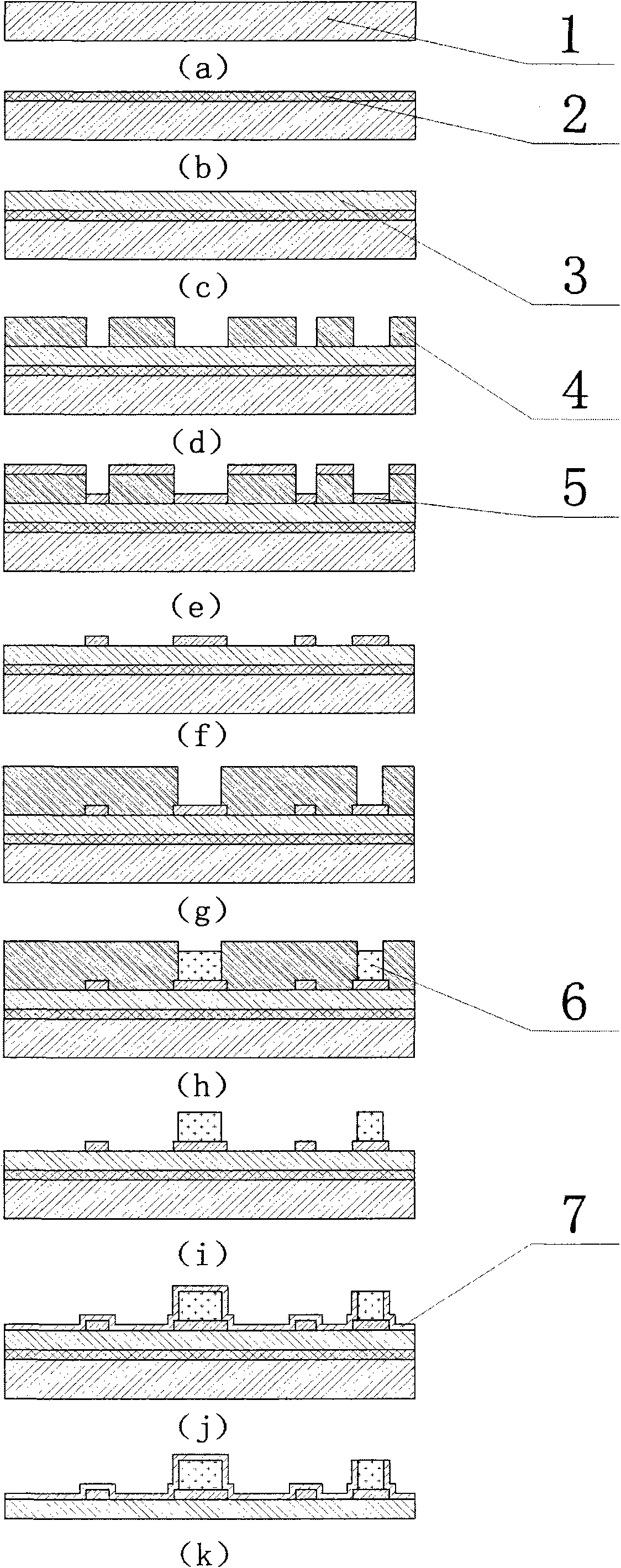
[0034] This embodiment proposes a method for making a nickel (Ni) metal flexible film resistor array on a flexible substrate, which specifically includes the following steps:
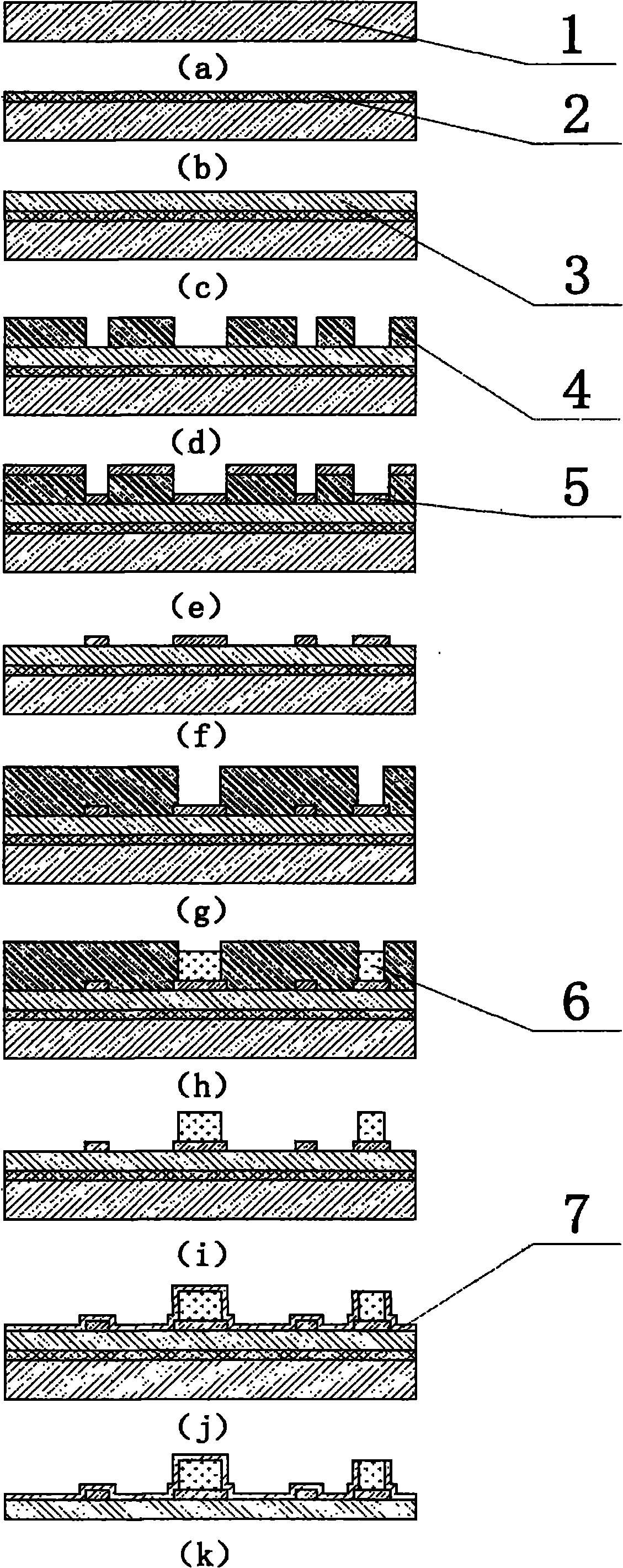
[0035] Step 1: Clean the silicon wafer 1, remove the surface native oxide layer and organic contamination, and then dry it, such as figure 1 (a);
[0036] Step 2: Sputter a 1 micron metal chromium film as a sacrificial layer 2, such as figure 1 (b);
[0037] Step 3: Using the method of multiple coatings, spin-coat the PI prepolymer, and thermally cure it under the step-up temperature conditions required by the PI prepolymer to form a 20-micron PI film layer 3, such as figure 1 (c).
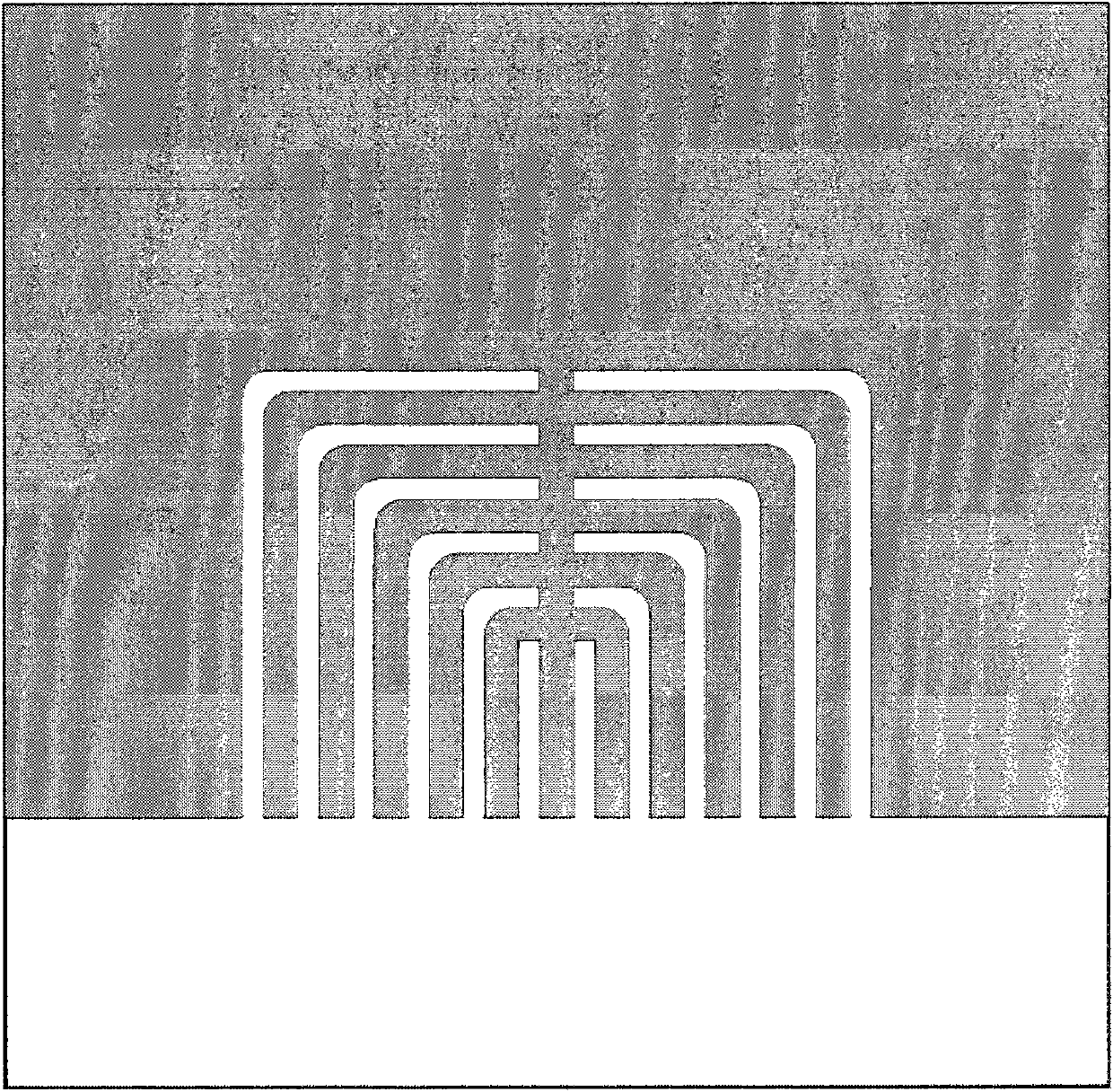
[0038] Step 4: Spin-coat the positive photoresist BP EPG533, and perform photolithography and development on it. The pattern of the photoresist used is as follows figure 2 , so that the pattern of the thermistor array and its electrical connection is defined on the photoresist pattern layer 4, such as figure 1 (d);
...
Embodiment 2
[0047] This embodiment proposes a method for fabricating a platinum metal flexible thin film resistor array on a flexible substrate, which specifically includes the following steps:
[0048] Step 1: Clean the silicon wafer 1, remove the surface native oxide layer and organic contamination, and then dry it, such as figure 1 (a);
[0049] Step 2: sputtering 800 nanometers of metal aluminum (thin film as sacrificial layer 2, such as figure 1 (b);
[0050]Step 3: Using the method of multiple coatings, spin-coat the PI prepolymer, and thermally cure it under the step-up temperature conditions required by the PI prepolymer to form a PI film 3 of 35 microns, such as figure 1 (c).
[0051] Step 3: Spin-coat the positive photoresist S1818, and perform photolithography and development on it. The pattern of the photolithography plate used is as follows Figure 4 , so that the pattern of the thermistor array and its electrical connection is defined on the photoresist pattern layer 4, ...
PUM
 Abstract
Description
Claims
Application Information


