Windowing process of solar crystalline silicon battery

A technology of crystalline silicon battery and window opening technology, which is applied in the direction of circuits, electrical components, sustainable manufacturing/processing, etc. Unstable window effect and other problems, to achieve the effect of low thickness uniformity, good applicability, and stable window opening

Active Publication Date: 2013-03-13
HENGDIAN GRP DMEGC MAGNETICS CO LTD
View PDF8 Cites 6 Cited by
  • Summary
  • Abstract
  • Description
  • Claims
  • Application Information

AI Technical Summary

Problems solved by technology

[0006] The purpose of the present invention is to solve the problems of large damage to the crystalline silicon substrate by the traditional laser window opening process, unstable window opening effect on silicon wafers with uneven thickness, and high requirements on the thickness uniformity of the deposited film on the ba

Method used


Image

  • Windowing process of solar crystalline silicon battery
  • Windowing process of solar crystalline silicon battery
  • Windowing process of solar crystalline silicon battery

Examples


Embodiment 1

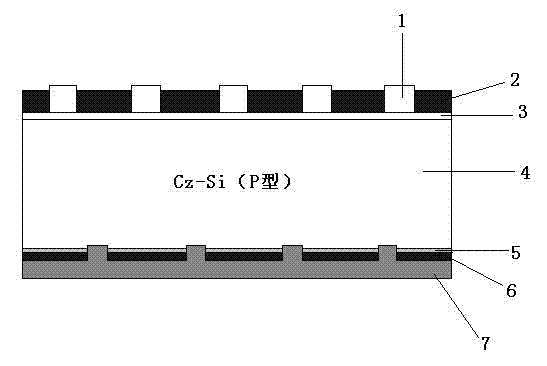
[0031] (1) Front-end process: Firstly, monocrystalline silicon wafers are placed in a NaOH solution with a mass concentration of 1.2% at 80°C for 15 minutes to form a pyramidal textured structure on the front and back sides, which are then cleaned with pure water and dried; Phosphorus is diffused on the front side of the chip to form an emitter (prior art), and the diffusion resistance is 70R 方 ; With a concentration of 7% HF solution, the phosphosilicate glass on the surface of the silicon wafer is cleaned and dried; then a layer of nitride is deposited on the front of the silicon wafer by PECVD (enhanced plasma vapor deposition method, prior art) Silicon anti-reflection coating with a thickness of 75nm and a refractive index of 2.0;

[0032] (2) Backside polishing: Put the silicon wafers processed in step (1) into the silicon wafer basket, put them into the polishing solution in the chemical polishing tank for chemical polishing for 5 minutes, the chemical polishing temperat...

Embodiment 2

[0038] (1) Front-end process: Firstly, monocrystalline silicon wafers are placed in a NaOH solution with a mass concentration of 1.2% at 80°C for 15 minutes to form a pyramidal textured structure on the front and back sides, which are then cleaned with pure water and dried; Phosphorus is diffused on the front side of the chip to form an emitter (prior art), and the diffusion resistance is 70R 方 ; With a concentration of 7% HF solution, the phosphosilicate glass on the surface of the silicon wafer is cleaned and dried; then a layer of nitride is deposited on the front of the silicon wafer by PECVD (enhanced plasma vapor deposition method, prior art) Silicon anti-reflection coating with a thickness of 75nm and a refractive index of 2.0;

[0039] (2) Backside polishing: Put the silicon wafers processed in step (1) into the silicon wafer basket, put them into the polishing solution in the chemical polishing tank for chemical polishing for 5 minutes, the chemical polishing temperat...

Embodiment 3

[0051] The difference between this embodiment and Example 1 lies in the formula of the etching slurry: the content of each component in the etching slurry is: concentrated phosphoric acid 15%, terpineol 8%, ethyl cellulose 12%, graphite powder 35% %, polyethylene glycol 30%. Others are with embodiment 1.


PUM

PropertyMeasurementUnit
Thicknessaaaaaaaaaa
Thicknessaaaaaaaaaa
Thicknessaaaaaaaaaa

Abstract

The invention discloses a windowing process of a solar crystalline silicon battery and aims at solving problems that traditional laser windowing processes are large in damages to crystalline silicon substrates, unstable in windowing effects of silicon chips with uneven thicknesses and high in eveness requirements of thicknesses of back deposition films. According to the windowing process of the solar crystalline silicon battery, a chemical etching method is used for windowing, the selectivity is high, damages to the silicon chips are absent, the applicability is good, the windowing effects on the silicon chips with uneven thicknesses are stable, and eveness requirements of the thicknesses of the back deposition films are low.

Description

technical field [0001] The invention relates to the technical field of solar crystal silicon cell production, in particular to a window opening process for solar crystal silicon cells. Background technique [0002] On the surface of the silicon wafer, the periodicity of the crystal is destroyed to generate dangling bonds, so that there are a large number of defect levels in the band gap on the crystal surface; in addition, dislocations, chemical residues, and deposition of surface metals will all introduce defect levels. These make the surface of the silicon wafer a recombination center. In order to reduce the production cost, people continue to reduce the thickness of the silicon wafer, so that the photogenerated carriers can easily diffuse to the back surface and increase the recombination of the back surface. There are two basic techniques for reducing the recombination rate on the surface of a solar cell. One is to reduce the surface state density, the surface recombin...

Claims


Application Information

Patent Timeline
IPC IPC(8): H01L31/18
CPCY02P70/50
Inventor 韩健鹏陈金灯吴敏吕绍杰
Owner HENGDIAN GRP DMEGC MAGNETICS CO LTD
Why Eureka
Try Eureka