Photoetching manufacturing process

A production process and photolithography technology, applied in the field of photolithography and etching production process, can solve problems such as photoresist peeling off, achieve the effect of improving wafer yield and preventing acid tank pollution

Inactive Publication Date: 2011-01-26
SEMICON MFG INT (SHANGHAI) CORP +1
View PDF0 Cites 19 Cited by
  • Summary
  • Abstract
  • Description
  • Claims
  • Application Information

AI Technical Summary

Problems solved by technology

[0004] In order to overcome the problem that the photoresist is easy to fall off during the wet etching process in the prior art, the present invention provides a process that can ensure the etching precision and is beneficial to metal filling

Method used


Image

  • Photoetching manufacturing process
  • Photoetching manufacturing process
  • Photoetching manufacturing process

Examples


Embodiment Construction

[0016] The photolithography manufacturing process of the present invention will be further described in detail below in conjunction with the accompanying drawings and specific embodiments.

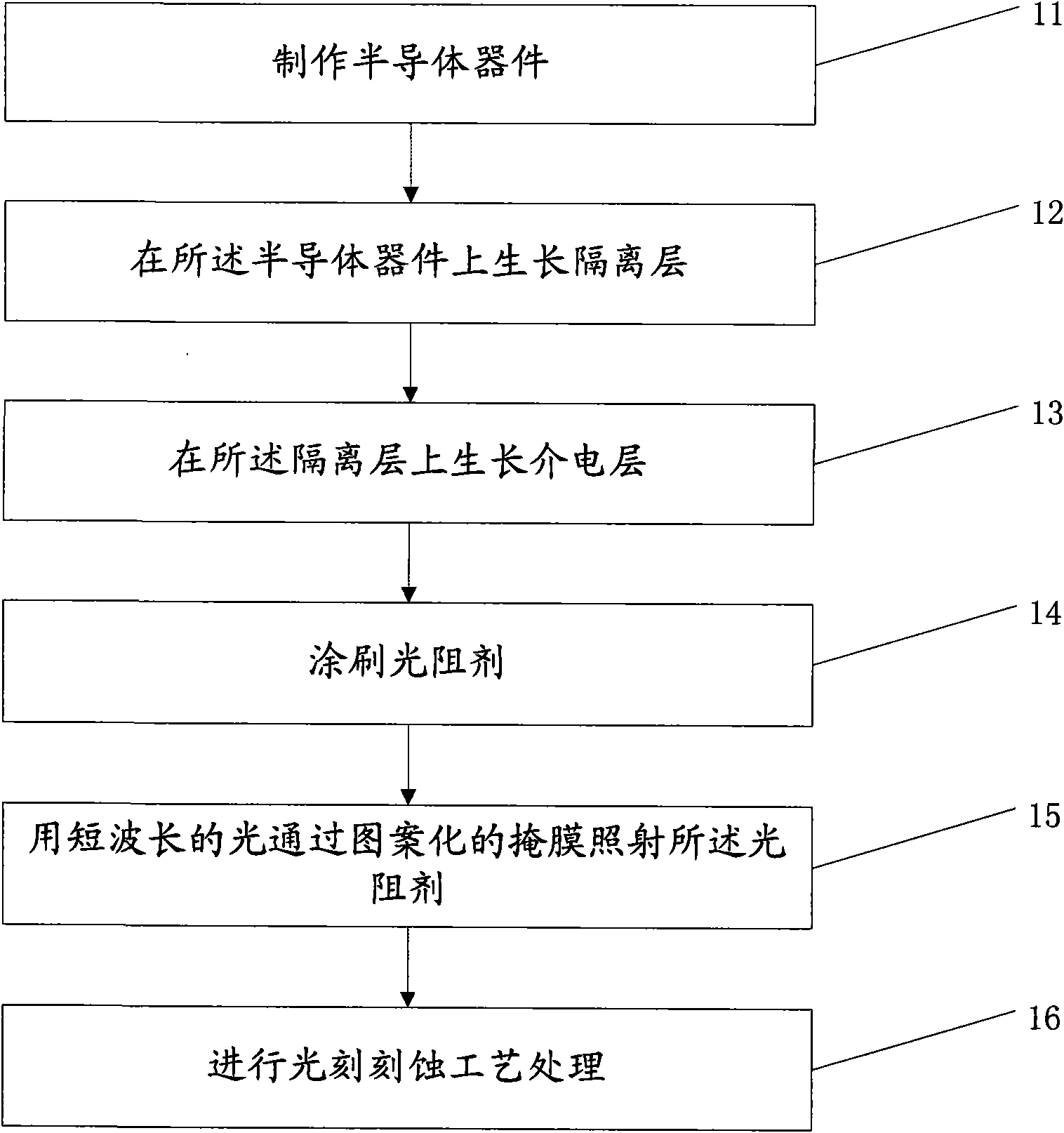
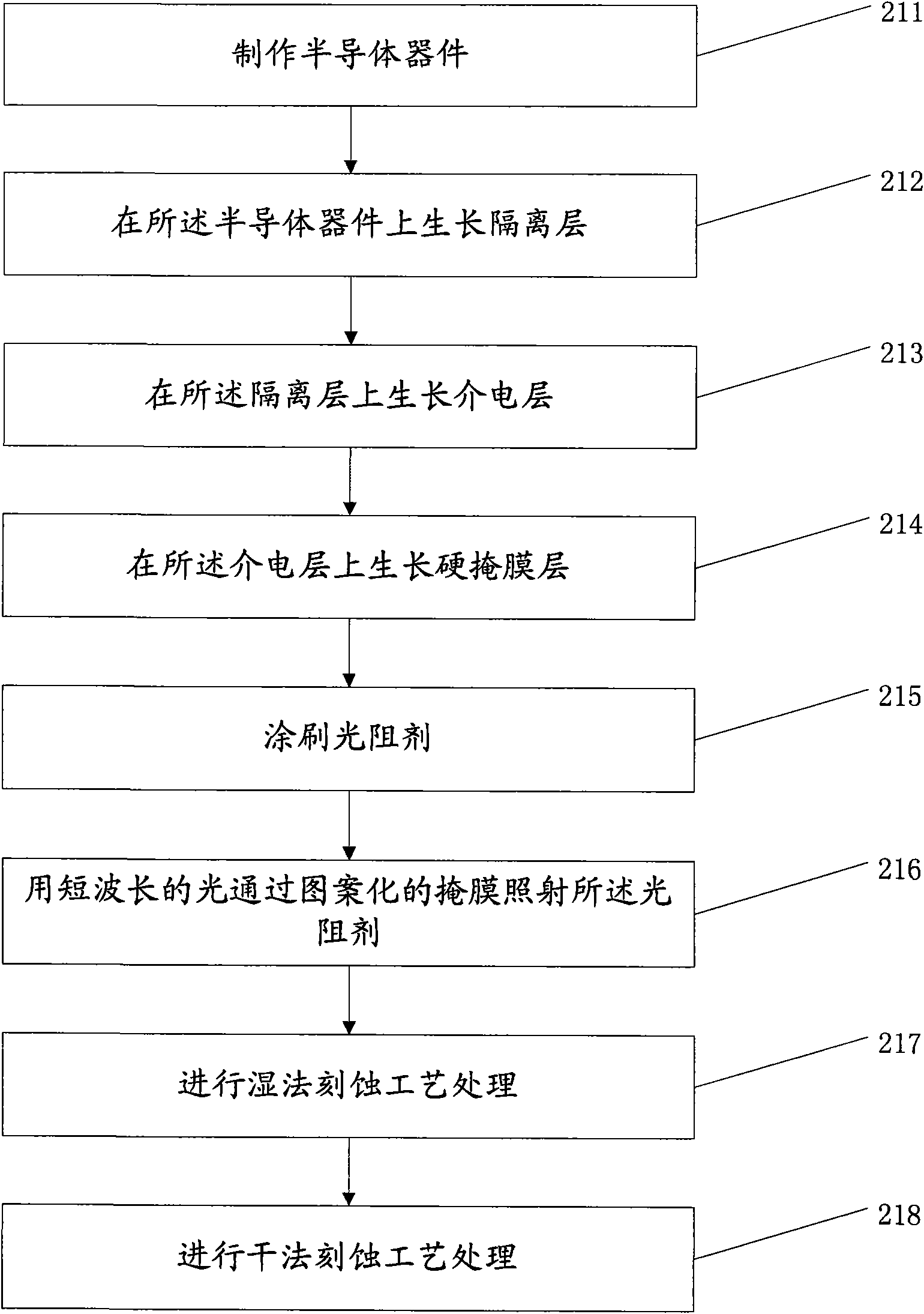
[0017] First, please refer to figure 2 , figure 2 It is a flow chart of the etching process of the present invention, including the following steps: Step 211: making a semiconductor device, including a series of processes such as film growth, etching, ion implantation and cutting on the wafer, until the semiconductor device is formed, according to different devices Types, using different manufacturing processes, not described one by one here; step 212: growing an isolation layer on the semiconductor device, the isolation layer material is ethyl silicate (TEOS), the function of the isolation layer is to The dielectric layer to be grown is isolated from the semiconductor device, because the dielectric layer generally contains boron and phosphorus, which are impurities relative to the semi...


PUM

PropertyMeasurementUnit
thicknessaaaaaaaaaa
thicknessaaaaaaaaaa

Abstract

The invention provides a photoetching manufacturing process which comprises the following steps of: manufacturing a semiconductor device, growing an isolating layer on the semiconductor device, growing a dielectric layer on the isolating layer, growing a hard mask layer on the dielectric layer, spreading photoresist, irradiating the photoresist by using short-wavelength light through a patterned mask, carrying out wet etching, and carrying out dry etching. The invention optimizes the prior art by using the photoetching manufacturing process and solves the problem of photoresist falling caused by limited adhesion ability between photoresist and dielectric in the process of wet etching.

Description

technical field [0001] The invention relates to a semiconductor process, in particular to a photoetching process. Background technique [0002] In many semiconductor processes, etching is one of the core process technologies that determine the feature size, and etching is divided into wet etching and dry etching. Wet etching is widely used in the semiconductor process, starting from cutting silicon ingots into semiconductor silicon wafers, chemical etchants are used for grinding and polishing to obtain optical-level flat and non-destructive surfaces, during thermal oxidation and epitaxial growth Prior to this, semiconductor silicon wafers were chemically cleaned to remove contamination from handling and storage. Wet etching is especially suitable for surface etching of polysilicon, oxides, nitrides and metals. In the current semiconductor process, a very important application of wet etching is the etching in the wafer double gate oxide process. , including high-voltage gat...

Claims


Application Information

Patent Timeline
Patent Type & Authority Applications(China)
IPC IPC(8): H01L21/02H01L21/311G03F7/20
Inventor 马飞杨晨任晓梅
Owner SEMICON MFG INT (SHANGHAI) CORP
Why Eureka
Try Eureka