Nanostructured thermoelectric material and device and production method thereof

A thermoelectric material and nanostructure technology, which is applied in the manufacture/processing of thermoelectric devices, thermoelectric device parts and other directions, can solve the problems of poor thermal stability and difficult deviceization, and achieve the effect of improving performance and crystallinity.

Inactive Publication Date: 2011-02-09
SUN YAT SEN UNIV
View PDF8 Cites 6 Cited by
  • Summary
  • Abstract
  • Description
  • Claims
  • Application Information

AI Technical Summary

Problems solved by technology

[0018] In order to solve the above-mentioned deficiencies and shortcomings of existing nanostructured thermoelectric materials that are not easy to be deviceized and have poor thermal stability, the primary purpose of the present invention is to provide a nanostructured thermoelectric material with good thermal stability

Method used


Image

  • Nanostructured thermoelectric material and device and production method thereof
  • Nanostructured thermoelectric material and device and production method thereof
  • Nanostructured thermoelectric material and device and production method thereof

Examples


Embodiment 1

[0049] Thermoelectric multilayer devices deposited using masked magnetron sputtering:

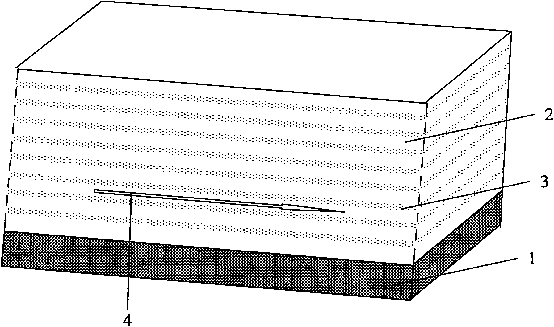
[0050] In this example, glass is used as the substrate, the bismuth-tellurium thermoelectric material is used as the thermoelectric layer, and the tungsten particle accumulation interface is used as the phonon scattering layer. The film deposition method is radio frequency magnetron sputtering, and the background vacuum is 1*10 -4 Pa, the working pressure is 0.7Pa.

[0051] The glass substrate was cleaned ultrasonically with acetone, alcohol and deionized water in sequence, and the substrate was blown dry with dry pure nitrogen.

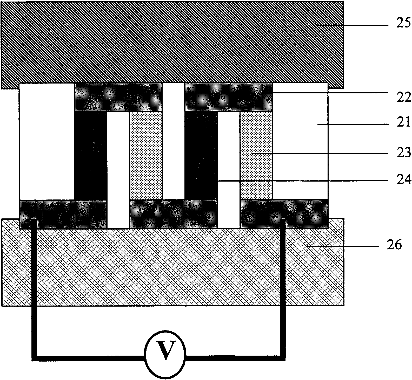
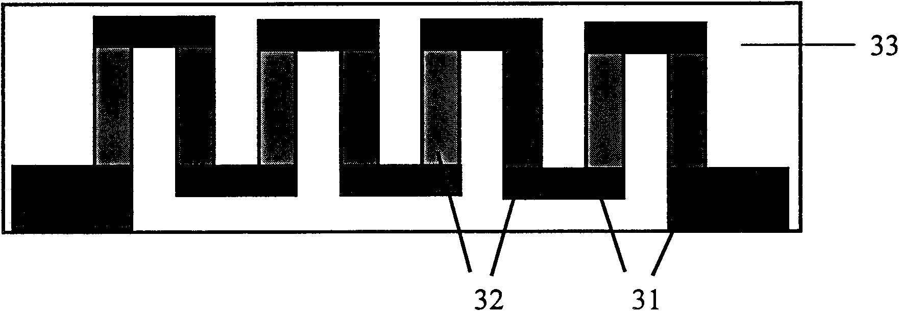
[0052] Cover the p-type thermoelectric arm mask on the substrate. Use radio frequency magnetron sputtering to coat a layer of p-type thermoelectric material with a power density of 1-10W / cm 2 , the thickness is 10nm, and then coated with a layer of tungsten particles, the power density can be 1~5W / cm 2 , the particle size is 5nm, the interface thickness is 5nm...

Embodiment 2

[0057] Thermoelectric multilayer devices deposited using masked magnetron sputtering:

[0058] The mica is used as the substrate, the bismuth-tellurium series thermoelectric material is used as the thermoelectric layer, and the silicon dioxide particle accumulation interface is used as the phonon scattering layer. The film deposition method is radio frequency magnetron sputtering, and the background vacuum is 1*10 -4 Pa, the working pressure is 0.1-2Pa.

[0059] The mica substrate was ultrasonically cleaned with acetone, alcohol, and deionized water in sequence, and the substrate was blown dry with dry pure nitrogen.

[0060] Cover the p-type thermoelectric arm mask on the substrate. Use radio frequency magnetron sputtering to coat a layer of p-type thermoelectric material with a power density of 2W / cm 2 , the thickness is 100nm, and then coated with a layer of silica particles, the power density is 2W / cm 2 , the particle size is 5nm, the interface thickness is 5nm, this pro...

Embodiment 3

[0065] Thermoelectric multilayer devices deposited using masked magnetron sputtering:

[0066] In this example, mica is used as the substrate, the cobalt-antimony series thermoelectric material is used as the thermoelectric layer, and the tungsten particle accumulation interface is used as the phonon scattering layer. The film deposition method is radio frequency magnetron sputtering, and the background vacuum is 1*10 -4 Pa, the working pressure is 0.1-2Pa.

[0067] The mica substrate was ultrasonically cleaned with acetone, alcohol, and pure water in sequence, and the substrate was blown dry with dry pure nitrogen.

[0068] Cover the p-type thermoelectric arm mask on the substrate. Use radio frequency magnetron sputtering to coat a layer of p-type thermoelectric material with a power density of 0.1W / cm 2 , the thickness is 5nm, and then coated with a layer of tungsten particles, the power density is 0.1W / cm 2 , the particle size is 1nm, the interface thickness is 1nm, thi...


PUM

PropertyMeasurementUnit
thicknessaaaaaaaaaa
thicknessaaaaaaaaaa
particle sizeaaaaaaaaaa

Abstract

The invention discloses a nanostructured thermoelectric material, a nanostructured thermoelectric device and a production method thereof. The thermoelectric material comprises an insulating substrate and a nanostructured thermoelectric membrane, wherein the nanostructured thermoelectric membrane is composed of at least two nano-thickness thermoelectric material layers and at least two phonon scattering layers, and the thermoelectric material layers and the phonon scattering layers are overlapped alternately. The thermoelectric material can be a p-type thermoelectric material or an n-type thermoelectric material, which depends on the type of charge carrier of the thermoelectric material layers. Connecting electrodes are plated between the thermoelectric membranes of a p-type nanostructured thermoelectric material and a n-type nanostructured thermoelectric material so as to form a thermoelectric pair; and then a plurality of thermoelectric pairs are connected in parallel or in series so as to form the thermoelectric device. The nanostructured thermoelectric material of the invention has the advantages of good thermal stability, high nanostructured membrane deposition efficiency, high thermoelectric conversion efficiency, and lower cost; and the nanostructured thermoelectric device has the advantages of simple structure, easy preparation, low internal resistance, and great practical value in the fields such as refrigeration / calorification or temperature differential power generation, and the like.

Description

technical field [0001] The invention belongs to the field of thermoelectric conversion materials, and in particular relates to a nanostructure thermoelectric material, a device and a preparation method thereof. Background technique [0002] Thermoelectric materials are functional materials capable of direct heat-to-electricity and electricity-to-heat conversion. Power generation devices and refrigeration devices made of thermoelectric materials have the advantages of simple structure, light weight and no moving parts, so thermoelectric materials have great application value and incomparable in the field of energy and refrigeration. advantage. [0003] According to existing theories, the conversion efficiency of thermoelectric materials is determined by their ZT value. where Z is the thermoelectric figure of merit and T is the temperature used. The ZT of the material thermoelectric material can be expressed as, ZT=(S 2 σ / k)T, where T is the absolute temperature, S is the ...

Claims


Application Information

Patent Timeline
Patent Type & Authority Applications(China)
IPC IPC(8): H01L35/02H01L35/34
Inventor 任山叶志超李立强李义兵洪澜
Owner SUN YAT SEN UNIV
Why Eureka
Try Eureka