Low contamination, low energy beamline architecture for high current ion implantation

An ion implantation system, ion beam technology, applied in circuits, discharge tubes, electrical components, etc., can solve problems such as influence

Active Publication Date: 2011-04-13
AXCELIS TECHNOLOGIES
View PDF3 Cites 16 Cited by
  • Summary
  • Abstract
  • Description
  • Claims
  • Application Information

AI Technical Summary

Problems solved by technology

[0015] However, implementing a deceleration element into an ion implanter is strongly influenced by the configuration of that particular ion implanter

Method used


Image

  • Low contamination, low energy beamline architecture for high current ion implantation
  • Low contamination, low energy beamline architecture for high current ion implantation
  • Low contamination, low energy beamline architecture for high current ion implantation

Examples


Embodiment Construction

[0028] The present invention is now described with reference to the drawings, in which like reference numerals are used to refer to like elements, and in which structures illustrated are not necessarily drawn to this example.

[0029] The main aspect of the invention is to facilitate the realization of low pollution low energy beamline structures for high current injection.

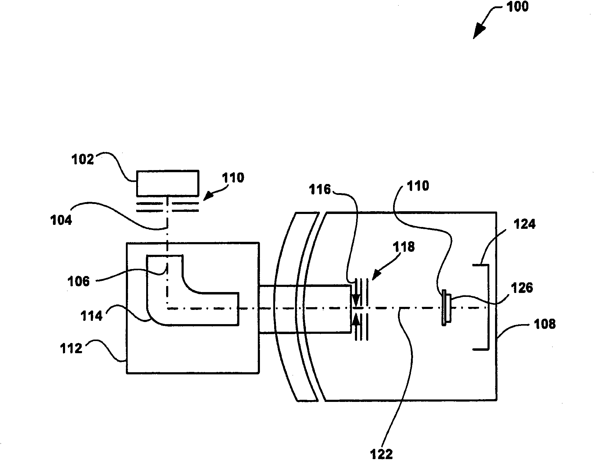
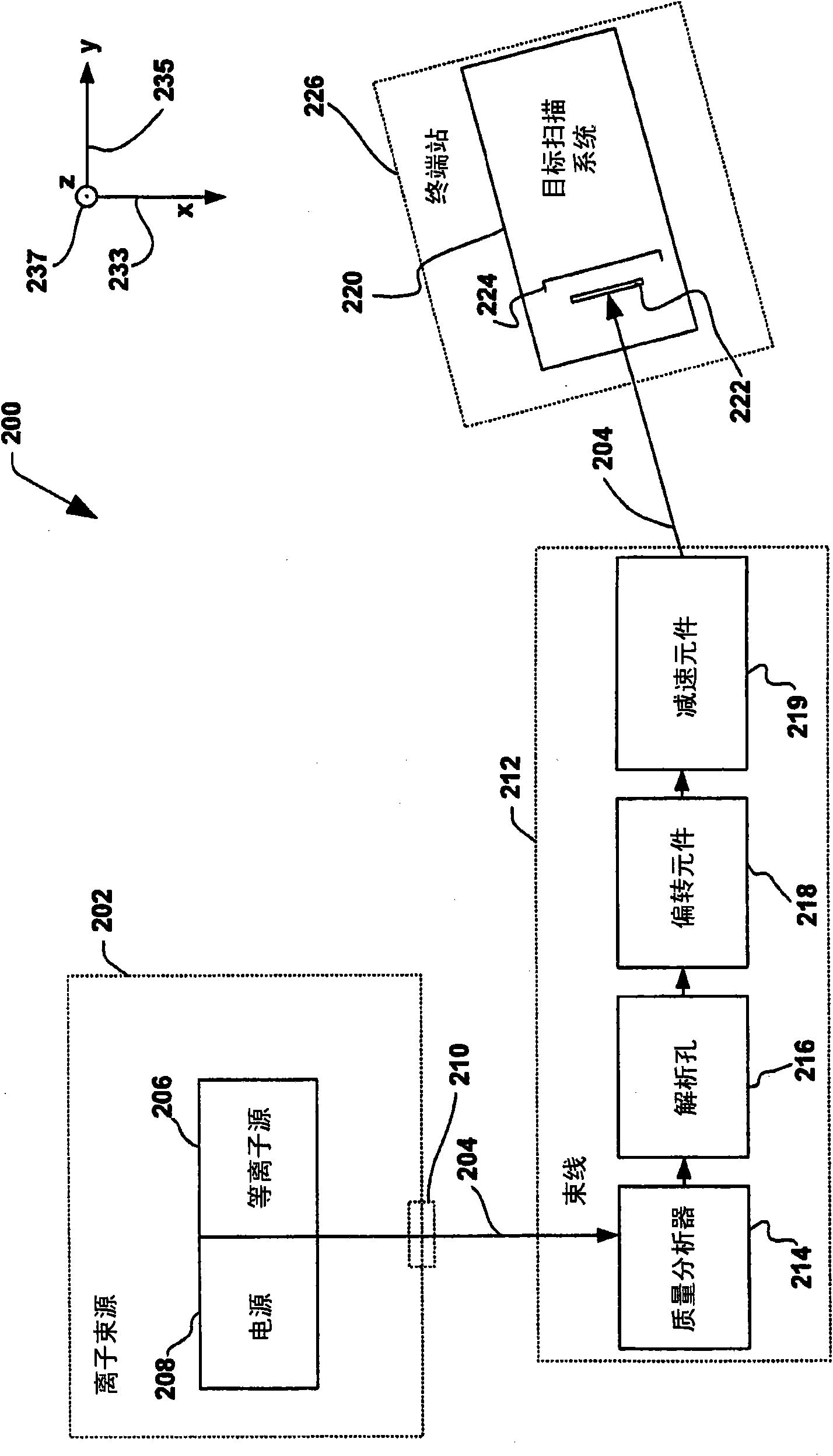
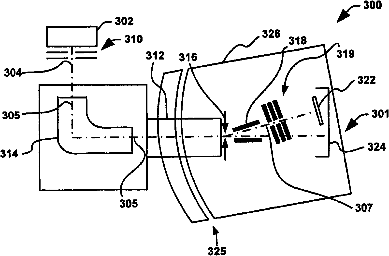
[0030] First, refer to figure 2 , which discloses a first embodiment of the present invention to provide an ion implantation system 200 comprising an ion source 202 for generating (eg pencil beam, ribbon beam, etc.) an ion beam 204 along a longitudinal beam path. The ion beam source 202 includes a plasma source 206 with an associated power supply 208 and an extraction device 210 . The extraction device can be of any design, by means of which it is possible, for example, to extract an elongated ribbon-shaped ion beam 204 with a large aperture ratio. The following examples are provided to more fully illus...


PUM


Abstract

An ion implantation system (500) comprising an ion source (502) that generates an ion beam (504) along a beam path (505, 507) a mass analyzer component (514) downstream of the ion source that performs mass analysis and angle correction on the ion beam, a resolving aperture (516) electrode comprising at least one electrode downstream of the mass analyzer component (514) and along the beam path having a size and shape according to a selected mass resolution and a beam envelope, a deflection element (518) downstream of the resolving aperture electrode that changes the path of the ion beam (507) exiting the deflection element, a deceleration electrode (519) downstream of the deflection element that decelerates the ion beam, a support platform within an end station (526) for retaining and positioning a workpiece (522) which is implanted with charged ions, and wherein the end station is mounted approximately eight degrees counterclockwise so that the deflected ion beam is perpendicular to the workpiece.

Description

technical field [0001] The present invention relates generally to ion implantation systems, and more particularly to systems and methods related to low-contamination, low-energy beamline configurations for high-current ion implanters. Background technique [0002] In the manufacture of semiconductor devices, ion implantation is used to dope semiconductors with impurities or dopants. An ion beam implanter is used to impinge a silicon wafer with an ion beam to make n or p-type extrinsic material doping or to form a passivation layer during integrated circuit fabrication. When used to dope semiconductors, the ion beam implanter implants selected exoplasmic ion species to produce the desired semiconductor material. Reference is first made to the conventional ion implantation system 100 of the prior art FIG. 1 . Implanting ions from a source material such as antimony, arsenic, or phosphorous produces an "n-type" wafer of exogenous material; while if a "p-type" wafer of exogenou...

Claims


Application Information

Patent Timeline
Patent Type & Authority Applications(China)
IPC IPC(8): H01J37/317
CPCH01J2237/022H01J2237/05H01J2237/24528H01J37/3007H01J2237/202H01J37/3171H01J37/20H01J37/317H01L21/265H10N15/10
Inventor Y·黄
Owner AXCELIS TECHNOLOGIES
Why Eureka
Try Eureka