A method for reducing the number of impurity particles in metal layer sputtering process

A technology of metal layer and sputtering, which is applied in metal material coating process, sputtering coating, coating, etc., can solve the problem of increasing the adhesion between metal titanium and titanium nitride, not mentioning the yield rate of metal bumps, increasing Manpower and material costs and other issues, to achieve the effect of reducing the generation rate of impurity particles, reducing labor and material costs, and increasing production capacity

Active Publication Date: 2017-07-14
NANTONG FUJITSU MICROELECTRONICS
View PDF2 Cites 0 Cited by
  • Summary
  • Abstract
  • Description
  • Claims
  • Application Information

AI Technical Summary

Problems solved by technology

Although this method is feasible, it seriously affects the production capacity of the sputtering machine, and at the same time increases the cost of manpower and materials. It can be seen that the operation of frequently stopping operations for cleaning has become a major technical problem that limits the increase in production capacity.
[0004] Chinese patent 03123734.7 discloses a sputtering device and a method for manufacturing a metal layer / metal compound layer using the device, which can reduce the difference in temperature distribution in the reaction chamber, increase the adhesion between metal titanium and titanium nitride, and It can reduce the accumulation of titanium nitride particles; Chinese patent 200510070055.0 discloses a crystal seat design of a sputtering cleaning chamber and a method of metallization manufacturing process using the design. The method of this patent can avoid the increase of the wafer temperature and improve the aluminum The ability to add holes to metal wires; however, none of the above patents mentions the reduction in the yield of metal bumps caused by the deposition of attachments during the metal sputtering process and the method to solve this problem, let alone how to deal with frequent stoppages The large technical problem of limiting the increase in production capacity due to cleaning operations

Method used


Image

  • A method for reducing the number of impurity particles in metal layer sputtering process
  • A method for reducing the number of impurity particles in metal layer sputtering process

Examples


Embodiment approach 1

[0023] Now in conjunction with the metal layer sputtering process and the plasma etching process, the technical scheme of the present invention is described in detail. The metal layer sputtering is to input an inert gas (such as argon) under vacuum conditions. Under the effect of high-voltage direct current, the argon is Ionization, argon ions hit the metal source (target), sputter out metal atoms, deposit and attach to the plated part, that is, form a metal layer.

[0024] Before the metal layer is sputtered, the plasma etching process must be carried out. There are usually two high-frequency power sources in the cavity of the plasma etching; one is a 2.0MHz microwave (Microwave) power supply, and the other is a 13.6MHz radio frequency (RF) power supply. )power supply. The microwave power supply exists above the plasma etching chamber (far away from the wafer), and its function is mainly to generate a plasma source (generating positively charged argon ions), while the main pu...

Embodiment approach 2

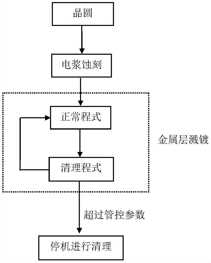
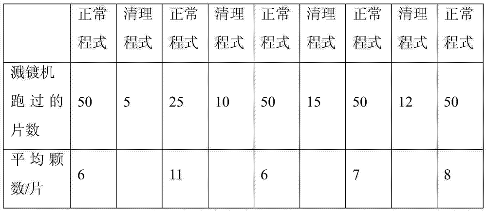
[0050] A method for reducing the number of impurity particles in a metal layer sputtering process, comprising the following steps: (1) turning on a microwave power supply and a radio frequency power supply, and performing plasma etching on a wafer surface and a metal pad surface; Metal layer sputtering on the wafer; (3) Set the upper limit parameter of particle number control, and stop the machine to clean the inner wall of the plasma etching chamber when this value is exceeded;

[0051] in,

[0052] The metal pad described in the step (1) is a gold pad, or a copper pad, or an aluminum pad; the plasma gas used in the plasma etching is argon;

[0053] Metal layer sputtering process comprises normal program and plasma etching cleaning program in the step (2);

[0054] The method adopted in the plasma etching cleaning program in the metal layer sputtering process described in step (2) is: turn off the radio frequency power supply, and use the plasma generated by the microwave po...


PUM


Abstract

The invention provides a method for decreasing the number of impurity particulates in the bumping metal layer sputtering process in the semiconductor packaging field. The method comprises the steps that (1) a microwave power supply and a radio-frequency power supply are turned on, and plasma etching is carried out on the surface of a wafer and the surface of a metal pad; (2) a sputtering machine carries out metal layer sputtering on the wafer; (3) the controlled upper limit parameter of the number of the particulates is set, and the sputtering machine is halted to clear the inner wall of a plasma etching cavity once the number of the particulates exceeds the controlled upper limit parameter. The metal layer sputtering process in the step (2) comprises a normal procedure and a plasma etching clearing procedure. By adopting the technical scheme, the number of the particulates is decreased, and the service life of the plasma etching cavity is prolonged, so that the maintenance frequency is reduced, and the labor cost and material cost are lowered; the generation rate of the impurity particulates in the bumping metal layer sputtering process is decreased by 60%, and the productivity of the sputtering machine is improved by 150%.

Description

technical field [0001] The invention relates to a metal layer sputtering process in a bump process in the field of semiconductor packaging, in particular to a method for reducing the number of impurity particles in the metal layer sputtering process. Background technique [0002] The production of tin-lead and tin-silver bumps is a necessary part of advanced semiconductor packaging (FC flip-chip packaging). Sputtering of the metal layer is usually the first step in the bumping process. The process flow of metal layer sputtering is to undergo plasma etching (or dry etching) before sputtering the metal layer. The purpose is to remove the oxide layer (aluminum pad or copper pad) on the opening of the long bump ( aluminum oxide or copper oxide), otherwise the contact resistance between the sputtered metal layer and the aluminum pad (or copper pad) will be too high and cause poor electrical properties. Plasma etching is to remove a layer of the wafer surface by plasma electric ...

Claims


Application Information

Patent Timeline
Patent Type & Authority Patents(China)
IPC IPC(8): H01L21/60C23C14/28
CPCC23C14/28H01L24/81H01L2224/81908
Inventor 丁万春
Owner NANTONG FUJITSU MICROELECTRONICS
Why Eureka
Try Eureka