

Preparation method of graphene thin film field emission material
A graphene thin film and field emission technology, applied in electrolytic coating, electrophoretic plating, coating, etc., can solve the problems that hinder the application of graphene and lack of preparation methods, and achieve low cost, good controllability, and easy scale-up Effect
- Summary
- Abstract
- Description
- Claims
- Application Information
AI Technical Summary
Problems solved by technology
Method used
Image

Examples
Embodiment 1
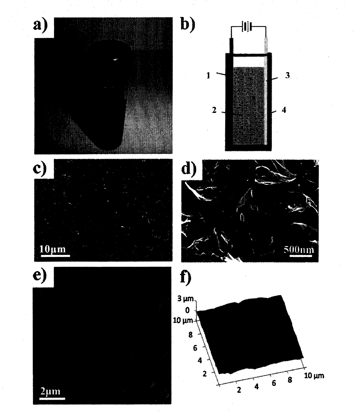
[0026] device attached figure 2 b, the stainless steel plate 1 is connected to the positive pole of the power supply, the ITO glass 3 is connected to the negative pole of the power supply, the graphene solution 2 is placed in a polymethyl methacrylate (PMMA) plastic container 4, and the stainless steel plate 1 and the ITO glass 3 are respectively inserted into the graphene solution 2 in.
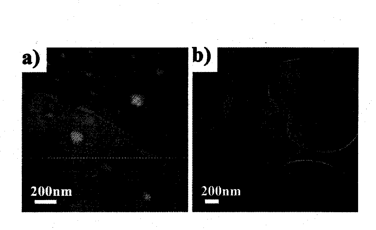
[0027] The lateral size prepared by chemical peeling method is 500nm~1μm, the number of layers is 1~3 layers (thickness is about 0.8~2.3nm), and the conductivity is 1×10 3 S / cm graphene is used as raw material, graphene and Mg(NO 3 ) 2 Add it to the low-polarity organic solvent isopropanol (IPA) in a weight ratio of 1:1, and the concentration of graphene is 0.1 mg·mL -1 , ultrasonically dispersed at room temperature for 1h to obtain a uniform and stable graphene suspension; a polished stainless steel plate was used as the positive electrode (5cm×2cm×2mm), and a conductive glass (2cm×2mm)...
Embodiment 2
[0030] device attached figure 2 b.
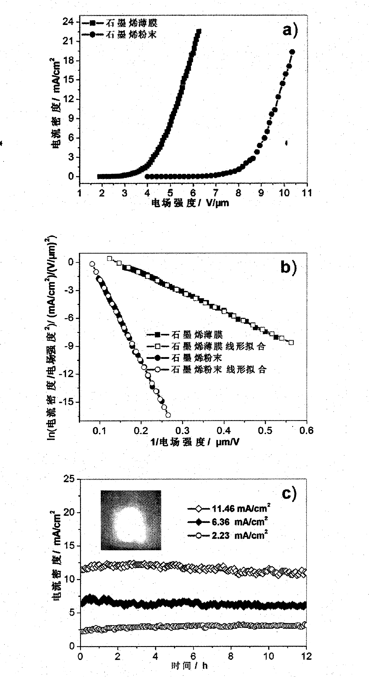
[0031] The lateral size prepared by chemical peeling method is 500nm~1μm, the number of layers is 1~3 layers (thickness is about 0.8~2.3nm), and the conductivity is 1×10³ S / cm graphene is used as raw material, graphene and Mg(NO 3 ) 2 Add it to the low polarity organic solvent isopropanol (IPA) in a weight ratio of 2:1, and the concentration of graphene is 0.2 mg·mL -1 , ultrasonically dispersed at room temperature for 2h to obtain a uniform and stable graphene suspension; a polished stainless steel plate was used as the positive electrode (5cm×2cm×2mm), and a conductive glass (2cm×2mm) coated with indium tin oxide (ITO) with a thickness of 120 μm was covered. 1cm×2mm) is the negative electrode, the distance between the positive and negative electrodes is 10mm, the operating voltage is 150V, the electrophoretic deposition time is 2min, and a graphene film with a thickness of about 1 μm is prepared; the electrophoretic deposition film (1c...
Embodiment 3
[0034] device attached figure 2 b.
[0035] The lateral size prepared by chemical peeling method is 500nm~1μm, the number of layers is 1~3 layers (thickness is about 0.8~2.3nm), and the conductivity is 1×10 3 S / cm of graphene as raw material, graphene and MgCl 2 Add it to the low-polarity organic solvent dimethylformamide (DMF) at a weight ratio of 1:1, and the concentration of graphene is 0.1 mg·mL -1 , ultrasonic dispersion at room temperature for 1h to obtain a uniform and stable graphene suspension; a polished stainless steel plate as the positive electrode (5cm × 2cm × 2mm), covered with a thickness of 200μm indium tin oxide (ITO) coated conductive glass (2cm × 1cm × 2mm) is the negative electrode, the distance between the positive and negative electrodes is 5mm, the operating voltage is 100V, the electrophoretic deposition time is 2min, and a graphene film with a thickness of about 0.5 μm is prepared; the electrophoretic deposition film (1cm×1cm×2mm) is used as a cold...
PUM
| Property | Measurement | Unit |
|---|---|---|
| Horizontal size | aaaaa | aaaaa |
| Thickness | aaaaa | aaaaa |
| Horizontal size | aaaaa | aaaaa |
Abstract
Description
Claims
Application Information