GaN blue light LED device using 3C-SiC-Si as substrate

An LED device, 3c-sic-si technology, applied in the direction of semiconductor devices, electrical components, circuits, etc., can solve the problems of high price, high crystallization temperature, reduce the area of ​​​​die light, and reduce production costs and processing. effect of cost

Inactive Publication Date: 2011-05-18
韩吉胜 +1
View PDF4 Cites 2 Cited by
  • Summary
  • Abstract
  • Description
  • Claims
  • Application Information

AI Technical Summary

Problems solved by technology

For example: Although the price of sapphire substrate is relatively low and the diameter of the wafer is large, its thermal conductivity is low, which makes it difficult to remove the heat generated during work; During the design of the electrical contact circuit, the front-end area of ​​the die must be used too much, thus reducing the area of ​​the die that can be used to emit light, and complicating the product manufacturing process
Using 4H/6H-SiC substrate, it is regrettable t

Method used


Image

  • GaN blue light LED device using 3C-SiC-Si as substrate
  • GaN blue light LED device using 3C-SiC-Si as substrate
  • GaN blue light LED device using 3C-SiC-Si as substrate

Examples


Embodiment Construction

[0023] The structure and manufacturing method of the present invention will be further described below in conjunction with the accompanying drawings.

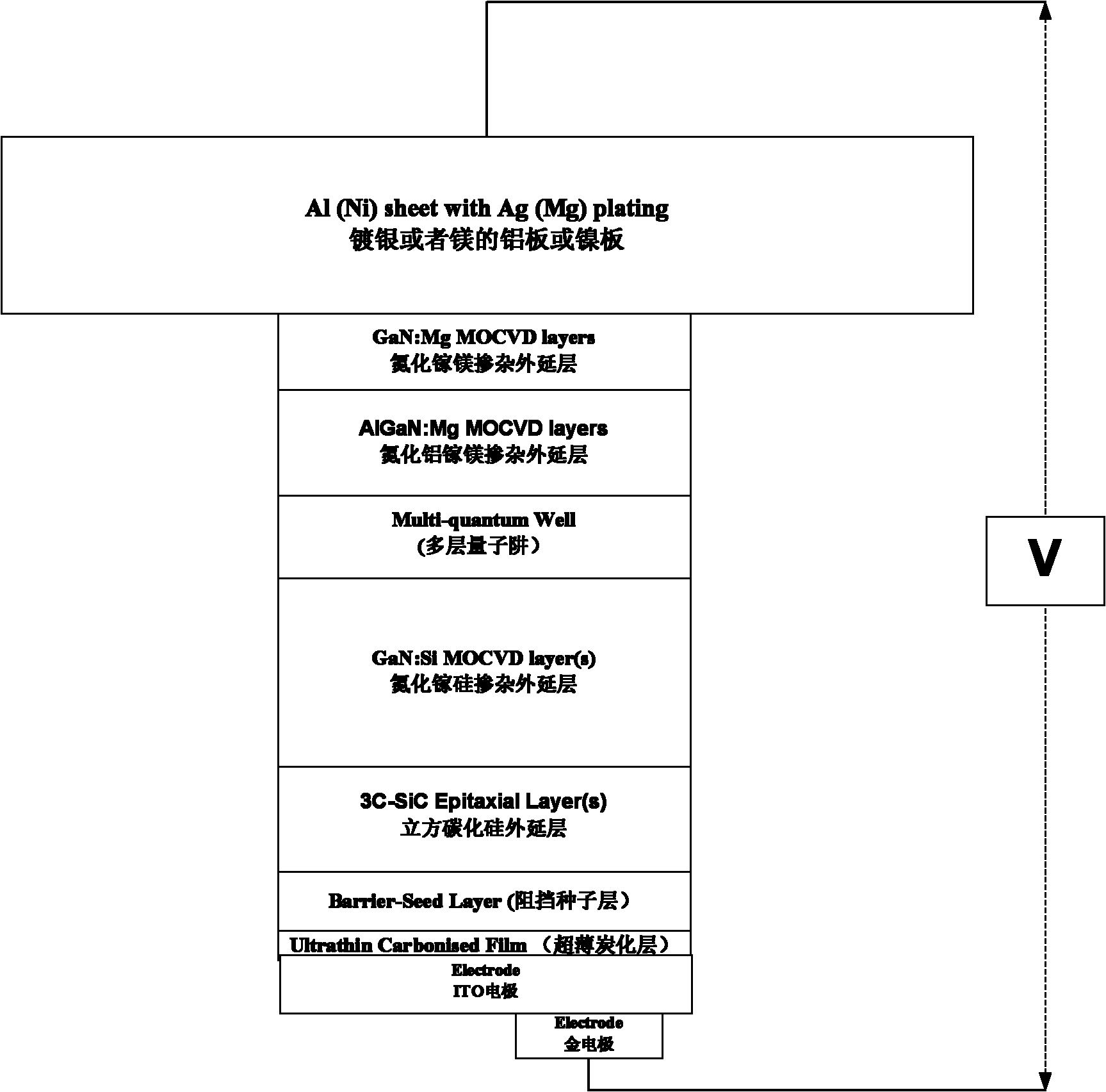
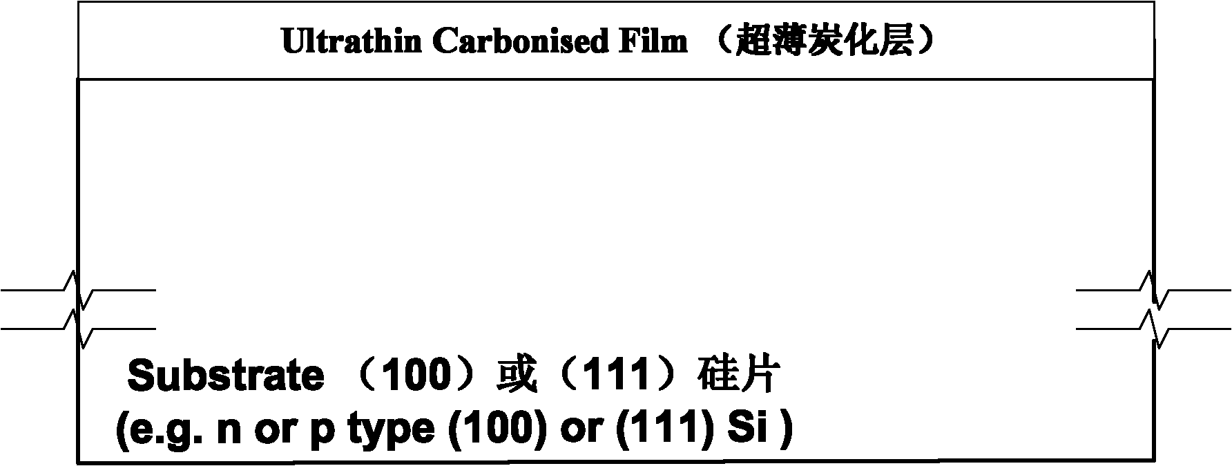
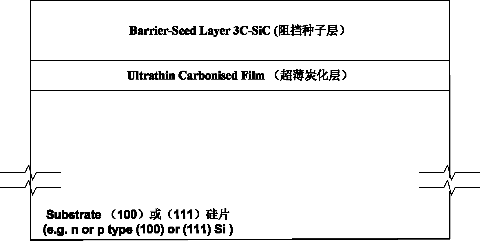
[0024] Referring to the accompanying drawings, the GaN blue LED device based on 3C-SiC-Si according to the present invention includes a base substrate layer, a buffer layer and a GaN structure layer from bottom to top, wherein the base substrate layer is made of silicon with a diameter of 50 mm to 300 mm. The buffer layer is a cubic silicon carbide epitaxial layer epitaxially grown on the silicon wafer, and the GaN structure layer is a GaN deposition layer epitaxially grown on the buffer layer.

[0025] A specific fabrication example of the method for fabricating the GaN blue LED device is as follows. This embodiment is a process step of manufacturing a GaN blue light LED device based on a six-inch silicon wafer.

[0026] In the first step, a six-inch n-type silicon wafer with a (111) crystal plane is selected as the basic sub...


PUM

PropertyMeasurementUnit
Diameteraaaaaaaaaa
Thicknessaaaaaaaaaa
Thicknessaaaaaaaaaa

Abstract

The invention relates to a GaN blue light light-emitting diode (LED) device using 3C-SiC-Si as a substrate. A manufacturing method comprises the following steps of: preparing a silicon wafer, manufacturing a buffer layer, which consists of an ultrathin carbonizing layer, a blocking seed layer and a cubic silicon carbide epitaxial layer, of the device on a silicon wafer serving as a basic substrate layer; depositing GaN on the buffer layer to form a GaN structural layer; bonding an aluminum plate or a nickel plate plated with silver or magnesium on the GaN structural layer to form ohmic contact; and etching silicon to form the GaN blue light LED device with a self-support structure. By the implementation and application of the technology of the invention, diameters of LEDs wafers are increased (which can reach 12 maximally), the production cost and machining cost of LED chip materials are reduced greatly, the high-quality GaN depositing layer can be obtained effectively and also can be used as barrier layer with high chemical stability to etch the silicon, and the opportunity is created for the improvement on LED tube cores, the extraction of light and the elimination of high-temperature stress.

Description

technical field [0001] The invention belongs to the technical field of manufacturing semiconductor devices, and relates to a GaN blue LED device with 3C-SiC-Si as a substrate and a manufacturing method thereof. Background technique [0002] In recent years, low-cost, clean, and energy-efficient solid-state light source LEDs technology has attracted great attention. LEDs are becoming a substitute for traditional light sources due to their low energy consumption and long lifespan. Gallium Nitride (GaN), was first used due to its excellent light emitting properties. GaN is usually epitaxially grown on non-identical substrates such as sapphire and 4H / 6H-SiC, but the characteristics of sapphire and 4H / 6H-SiC are not very ideal. For example: Although the price of sapphire substrate is relatively low and the diameter of the wafer is large, its thermal conductivity is low, which makes it difficult to remove the heat generated during work; During the design process of the electric...

Claims


Application Information

Patent Timeline
IPC IPC(8): H01L33/12H01L33/00
Inventor 韩吉胜徐现刚
Owner 韩吉胜
Why Eureka
Try Eureka