Ultra-wideband antenna

A technology of ultra-wideband antenna and microstrip line, which is applied in the direction of antenna, antenna grounding device, radiation element structure, etc. It can solve the problems of electromagnetic wave leakage, limited antenna bandwidth, and reduce system performance, so as to suppress unnecessary frequency bands and achieve good Impedance bandwidth and the effect of reducing the size of the antenna

Inactive Publication Date: 2011-05-18
HARBIN ENG UNIV
View PDF1 Cites 38 Cited by
  • Summary
  • Abstract
  • Description
  • Claims
  • Application Information

AI Technical Summary

Problems solved by technology

Usually this method will cause mismatch between the antenna and the microwave circuit, and even reduce the overall performance of the system, so designing an ultra-wideband antenna with notch characteristics is one of the important methods to solve this problem
At the same time, some shortcomings of the existing UWB antennas are solved: (1) Most of the current UWB antennas use microstrip monopole antennas or coplanar waveguide-fed monopole antennas, and the size of these antennas is relatively large
In recent years, although ultra-wideband antennas based on slot antennas can meet the application requirements of UWB (3.1GHz-10.6GHz), the feeding methods of these antennas are relatively complicated, which is not convenient for actual debugging and production
(2) At present, most ultra-wideband antennas usually need to drill holes during system integration, and use reactive elements to connect to the RF front-end, so the complexity of the system is increased, the performance of the system is reduced, and the needs of miniaturization cannot be met.
(3) Most of the current ultra-wideband antennas only meet the application requirements of UWB (3.1GHz-10.6GHz), and are not compatible with WLAN (2.4GHz-2.483GHz) applications
(4) In recent years, most of the ultra-wideband antennas with notch characteristics proposed by the academic circle mostly adopt the etching of various grooves on the ground plane and the radiation element to realize the notch characteristics, so the etching The slot will produce electromagnetic wave leakage and affect the radiation pattern of the antenna
[0003]Traditional printed ultra-wideband antennas are mainly conical antennas and printed disc-conical antennas. In order to reduce the volume, the Chinese patent "an ultra-wideband stepped floor printed monopole antenna , Application No. 2005100242288.7" describes an ultra-wideband antenna based on a stepped ground plate and an elliptical radiating element, but the bandwidth of the antenna is limited, which still cannot meet the application of UWB, and cannot overcome the electromagnetic interference problem of UWB and WLAN
The document "Harmonic Control For An Integrated Microstrip AntennaWith Loaded Transmission Line, Shun-Yun Lin, Kuang-Chih Huang, and Jin-Sen Chen. MicrowaveAnd Optical Technology Letters, Vol.44, No.4, February, 2005", proposed a Use periodic structure to suppress harmonics, use additional periodic filter structure to generate notch characteristics, realize UWB and WLAN cooperative work, but the volume is large and the structure is complex
In order to overcome the above-mentioned shortcomings, the document "Design of a 5.8-GHz Antenna Incorporating a NewPatch Antenna, Ching-Hong K.Chin, Quan Xue, Chi Hou Chan, IEEE Antennas And Wireless Propagation, Vol.4, 2005", expounds the coplanar The method of etching the filter on the waveguide feed signal line produces the characteristics of the notch, but the volume is still large, which cannot well realize the miniaturization design of the system, and the production requirements of the antenna are relatively high
Literature "A miniaturized monopole antenna for ultra-wide band applications with band-notch Filter, B. Ahmadi, R. Faraji-Dana, IET Microw. Antennas Propag., 2009, Vol.3, No.14, pp.1224-1231 .” described the ultra-wideband antenna with notch characteristics etched U-shaped groove and V-shaped groove, but the volume is large, and the gradual feeding structure is adopted, which brings inconvenience to design and debugging

Method used


Image

  • Ultra-wideband antenna
  • Ultra-wideband antenna
  • Ultra-wideband antenna

Examples


Embodiment 1

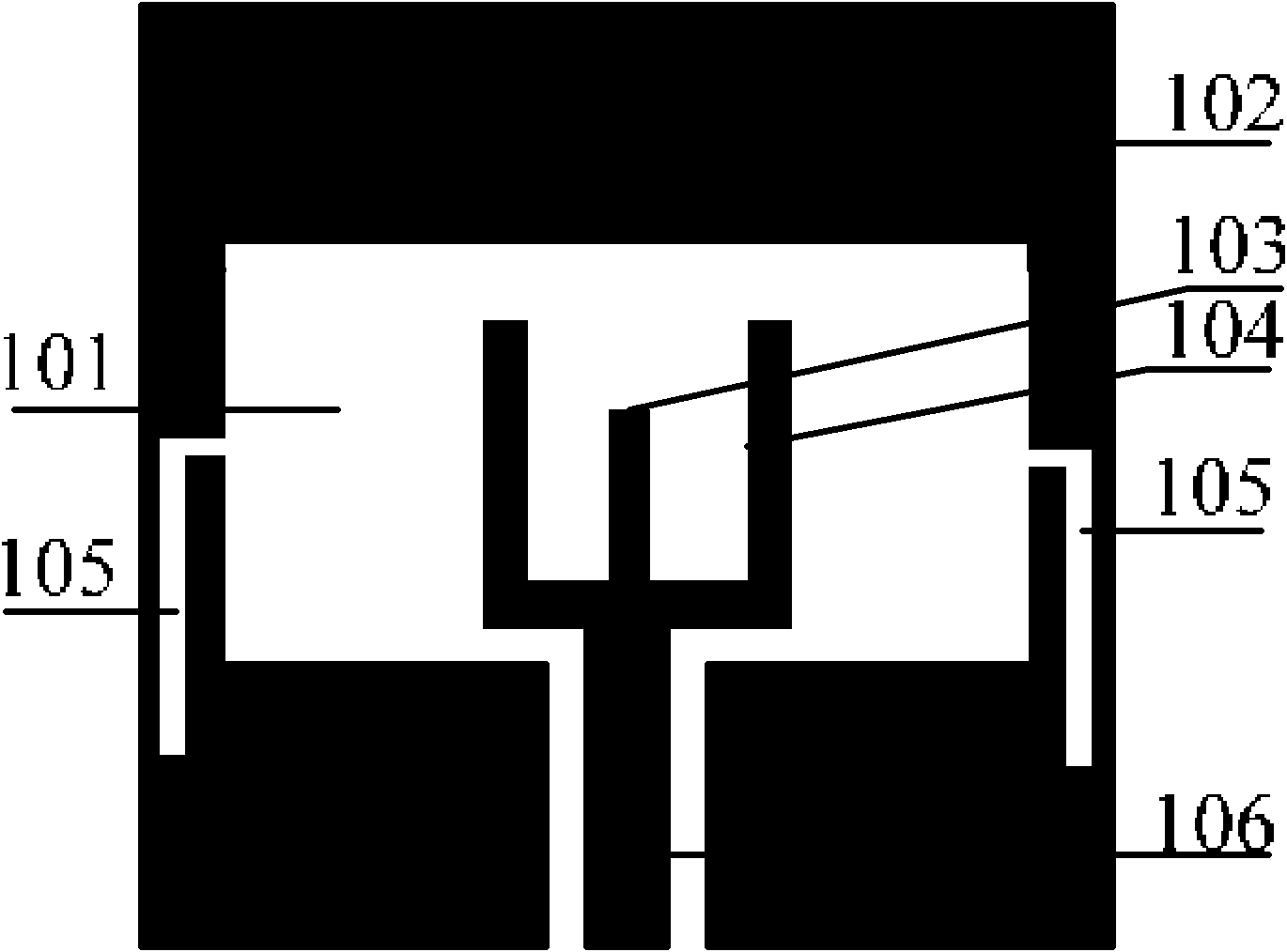
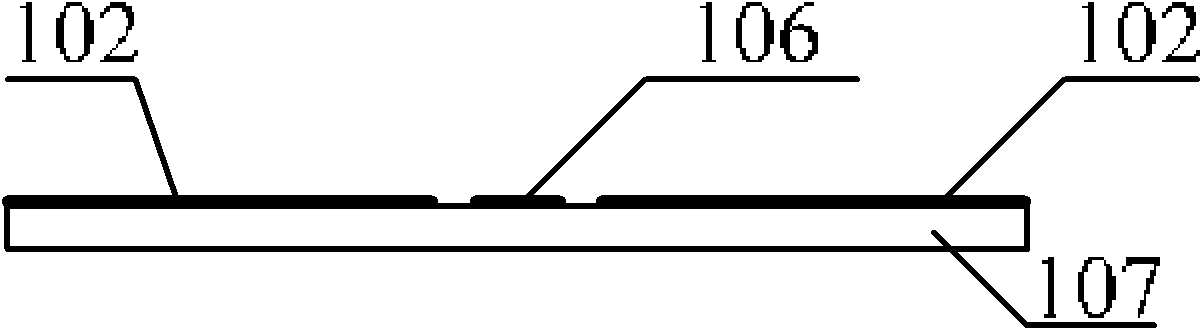
[0040] An example of the invention is figure 1 with figure 2 Shown. It is composed of a dielectric substrate 107, a radiation unit 104, a coplanar waveguide feeding signal strip line 106, a tuned microstrip line 103, a wide slot 101, two inverted L-shaped slots 105 and a coplanar waveguide ground plane 102. The lower end of the coplanar waveguide feeding signal strip line 106 of the antenna is connected to the SMA inner conductor. The outer conductor of the SMA is connected to the coplanar waveguide ground plane 102. according to figure 1 with figure 2 The structure shown can meet its ultra-wideband operating characteristics and notch characteristics as long as the appropriate size is selected.

[0041] Parameter setting:

[0042] 1. Tuning microstrip line

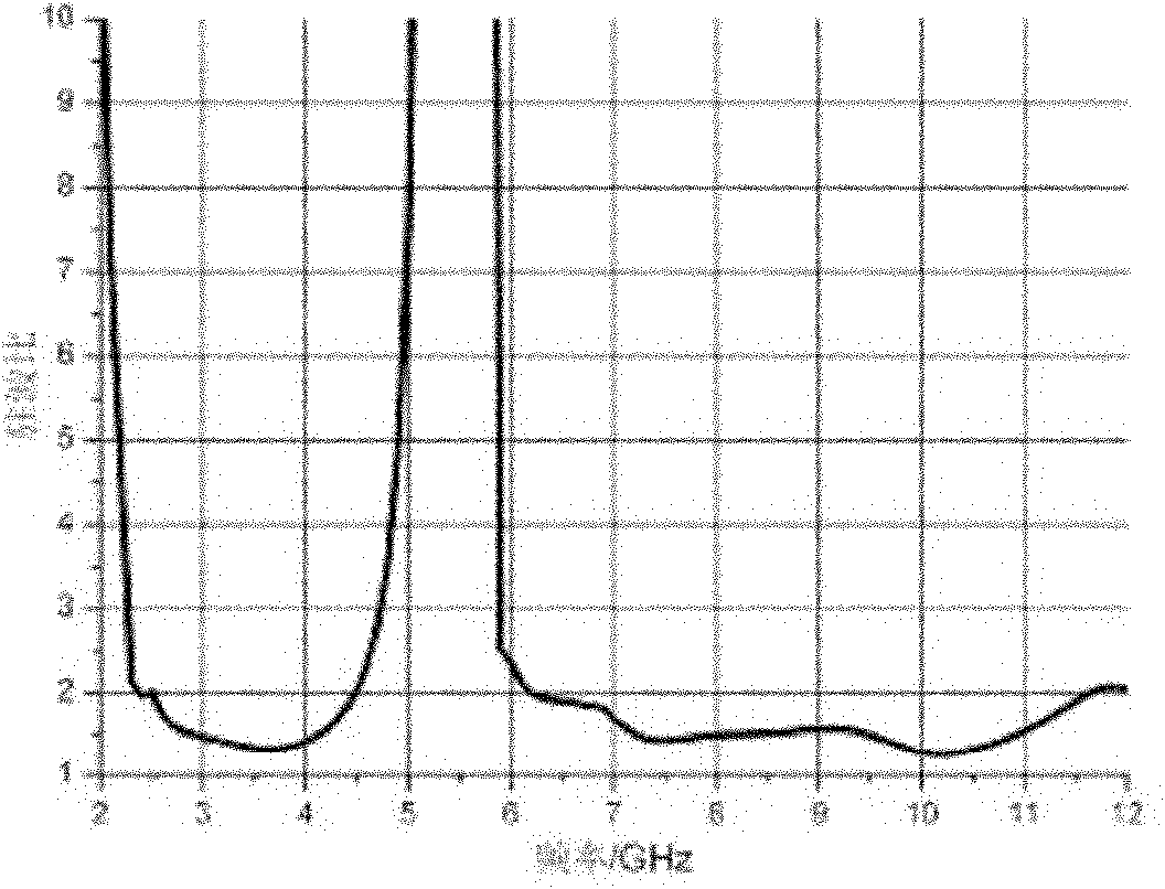
[0043] The notch characteristics of the antenna are mainly realized by inserting an open-circuit tuning microstrip line between the fork-shaped radiating elements. The tuning microstrip line is equivalent to a band rejection...

Embodiment 2

[0053] Such as Figure 7 As shown, another embodiment of the present invention is that the antenna does not have two inverted L-shaped slots, and the antenna radiating unit 204, the coplanar waveguide feeding signal strip line 206, the tuning microstrip line 203, and the wide slot 201 are composed. The entire antenna is printed on a dielectric substrate with a dielectric constant of 2.65. The lower end of the coplanar waveguide feeding signal strip line 206 of the antenna is connected to the SMA inner conductor. The outer conductor of the SMA is connected to the coplanar waveguide ground plane 202. according to Figure 7 The structure shown can meet its ultra-wideband operating characteristics and notch characteristics as long as the appropriate size is selected. The notch characteristics of the antenna are still realized by the tuning microstrip line. By adjusting the length and width of the tuning microstrip line, the center frequency of the notch and the bandwidth of the no...

Embodiment 3

[0055] Such as Picture 9 As shown, another embodiment of the present invention is that the radiating unit is directly composed of fork-shaped patches, without two inverted L-shaped grooves and tuning microstrip lines. The antenna radiation unit 304, a coplanar waveguide feeding signal strip line 306, and a wide slot 301 are composed. The entire antenna is printed on a dielectric substrate with a dielectric constant of 2.65. The lower end of the coplanar waveguide feeding signal strip line 306 of the antenna is connected to the SMA inner conductor. The outer conductor of the SMA is connected to the ground plane 302 of the coplanar waveguide. according to Picture 9 The structure shown can meet its ultra-wideband operating characteristics as long as the appropriate size is selected.


PUM


Abstract

The invention provides an ultra-wideband antenna. The ultra-wideband antenna comprises a dielectric substrate, wherein a radiation unit, a feeding structure and a ground plane are printed on the dielectric substrate; the radiation unit is a forked chip; the feeding structure is a coplanar waveguide feeding structure; and the ground plane is a coplanar waveguide ground plane. The ultra-wideband antenna has a coplanar waveguide structure, so that a single planar printed antenna structure can be realized; the ultra-wideband antenna can be easily integrated with a microwave integrated circuit; the coplanar waveguide ground plane can serve as the ground plane of the whole antenna, and particularly for the coplanar waveguide structure with a wideband slot structure, wideband work can be realized, and the electromagnetic interference of outside on the antenna can be effectively avoided; and wideband impedance bandwidth can be easily realized, and the efficiency of the antenna is improved, so that higher antenna gain can be achieved.

Description

technical field [0001] The invention relates to an ultra-wideband antenna, which can be used to receive and transmit radio waves. Background technique [0002] Since radio communication equipment and electronic information equipment are developing toward multi-functionality, miniaturization, ultra-wideband, and friendly coordination with the surrounding environment, this makes broadband, miniaturization, and high gain one of the hot research topics at home and abroad. In recent years, the coplanar waveguide structure that does not require drilling and is easy to integrate is changing day by day, and the structure can be fabricated by photography or photolithography, and has better polarization characteristics, so this technology has been applied in the design of ultra-wideband antennas and In the design of related microwave circuit components. However, the frequency band occupied by the current ultra-wideband communication and the wireless local area network have a common p...

Claims


Application Information

Patent Timeline
Patent Type & Authority Applications(China)
IPC IPC(8): H01Q1/38H01Q1/48H01Q13/08
Inventor 李迎松杨晓冬吴成云姜弢
Owner HARBIN ENG UNIV
Why Eureka
Try Eureka