Semiconductor laser device and method of manufacturing the device

A technology of a laser device and a manufacturing method, which is applied to semiconductor lasers, structures of optical waveguide semiconductors, lasers, etc., can solve problems such as deterioration of contact characteristics, damage to functions, changes in conductive characteristics of the laser exit end face, etc., and achieves low operating voltage, long Long life, high output effect

Inactive Publication Date: 2011-06-15
PANASONIC CORP
View PDF2 Cites 14 Cited by
  • Summary
  • Abstract
  • Description
  • Claims
  • Application Information

AI Technical Summary

Problems solved by technology

Therefore, based on the P of the area connected to the resistive P electrode + P + Type GaN contact layer / dielectric film interface determines the change of Fermi level, the resistance P electrode / P + Influenced by the Fermi level at the interface of the GaN-type GaN contact layer, there is a problem that the contact characteristics deteriorate
[0016] On the other hand, in the configuration described in Patent Document 2, although the above-mentioned problems do not occur, since the dielectric film material used as the end surface coating film is also covered by the current non-injection region during the end surface coating, it is accompanied by Changes in the stress characteristics of the dielectric film material, changes in optical properties such as the refractive index of the material, or changes in the stoichiometry of the material, and changes in the electrical conductivity of the laser emitting end surface, etc.
Therefore, since the structure in which the end surface coating film material is also used as the dielectric film in the current non-injection region impairs the function originally required for the dielectric film in the current non-injection region, there is a problem.

Method used


Image

  • Semiconductor laser device and method of manufacturing the device
  • Semiconductor laser device and method of manufacturing the device
  • Semiconductor laser device and method of manufacturing the device

Examples


Embodiment approach

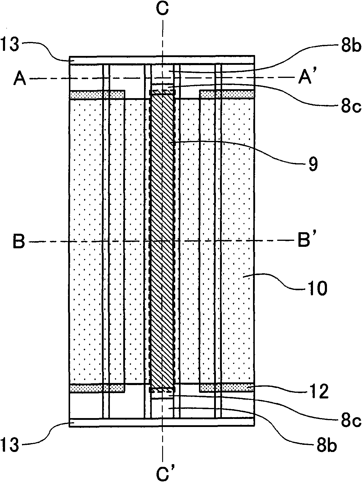
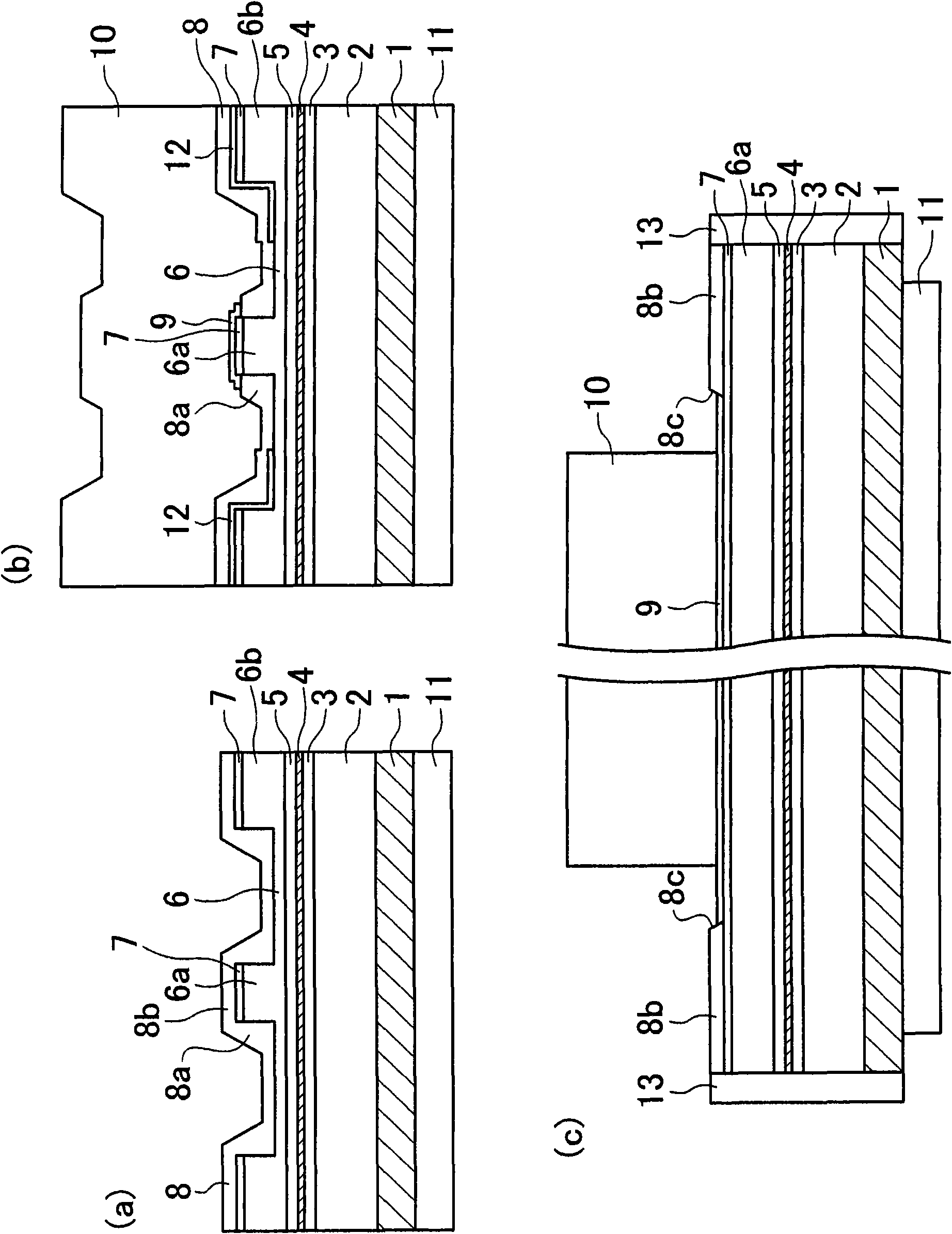
[0069] figure 1 It is a plan view showing the configuration of a semiconductor laser device according to one embodiment, specifically a GaN semiconductor laser diode, figure 2 (a) is figure 1 The cross-sectional view at the A-A' line (current non-injection area), figure 2 (b) is figure 1 The cross-sectional view at the B-B' line (current injection area) of figure 2 (c) is figure 1 The cross-sectional view at the C-C' line (the direction in which the ridge extends).

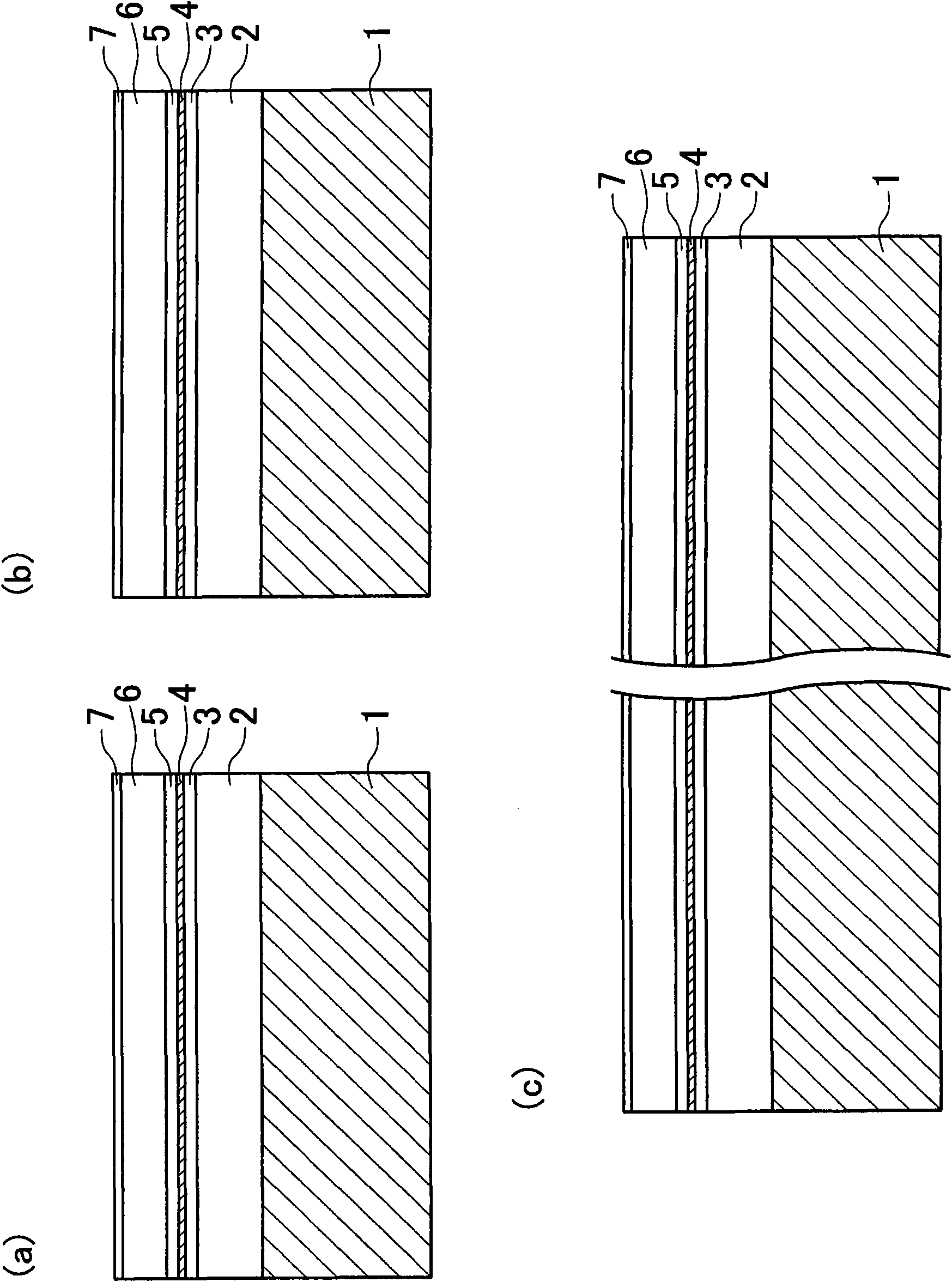
[0070] Such as figure 1 and figure 2 As shown in (a) to (c), on the n-type GaN substrate 1, for example, a layer made of n-type Al with a thickness of about 2.5 μm is formed. x Ga 1-x An n-type cladding layer 2 composed of N (x=0.03). On the n-type cladding layer 2, there is formed an n-type optical guiding layer 3 made of n-type GaN with a thickness of about 0.1 μm, for example. On the n-type photoguiding layer 3, a multiple quantum well active layer 4 is formed. The multiple quantum well activ...


PUM


Abstract

The present provides a semiconductor laser device achieving high output power, long life, and a low operation voltage and a method of manufacturing the device. A first semiconductor layer, an active layer, a second semiconductor layer, and a contact layer are sequentially stacked on a substrate. A ridge portion extending between both facets of a resonator is provided in the second semiconductor layer and the contact layer. A current confining layer is formed to be in contact with the ridge portion. The current confining layer has an opening on an upper surface of the ridge portion. A first electrode in contact with the contact layer is formed in the opening. A second electrode is provided on the first electrode. A non-current injection portion in contact with the contact layer is provided on the upper surface of the ridge portion near the resonator facet. The current confining layer and the non-current injection portion are formed of the same dielectric film. The second electrode is spaced apart from an upper surface region of the non-current injection portion.

Description

technical field [0001] The present invention relates to a semiconductor laser device and a manufacturing method thereof, and more particularly to a semiconductor laser device having an electrode structure utilizing a junction interface between a metal and a compound semiconductor having a work function different from the metal, and a manufacturing method thereof. Background technique [0002] In the source / drain electrodes of a high electron mobility field effect transistor (HEMT) using gallium arsenide (GaAs), which is a representative compound semiconductor narrow bandgap material, the metal is eutectically alloyed with a highly doped GaAs semiconductor layer, got resistive. On the other hand, the gate electrode has a structure utilizing a Schottky connection interface between a metal and a semiconductor. In recent years, in power devices using gallium nitride (GaN) and silicon carbide (SiC), which are widely researched and put into practical use, the source / drain electro...

Claims


Application Information

Patent Timeline
Patent Type & Authority Applications(China)
IPC IPC(8): H01S5/22H01S5/042H01S5/343
CPCB82Y20/00H01S5/2214H01S5/0425H01S5/0014H01S2301/02H01S5/0202H01S5/3211H01S5/22H01S5/34333H01S5/0601H01S5/04254H01S5/04252H01S2301/176
Inventor 工藤昭吉
Owner PANASONIC CORP
Why Eureka
Try Eureka