Conductive transparent copper-doped nickel oxide film and preparation method thereof

A conductive transparent nickel oxide technology, applied in the field of transparent electronics research, can solve the problems of restricting the application of TOS materials and the inability to synthesize transparent oxide pn junctions, etc., and achieve the effect of low equipment price, low price and simple operation

Inactive Publication Date: 2011-06-29
FUDAN UNIV
View PDF0 Cites 8 Cited by
  • Summary
  • Abstract
  • Description
  • Claims
  • Application Information

AI Technical Summary

Problems solved by technology

[0002] So far, the transparent oxide semiconductor (TransparentOxideSemiconductor, TOS) materials with continuously improved performance are all n-type semiconductors, and the corresponding p-type materials hav

Method used


Image

  • Conductive transparent copper-doped nickel oxide film and preparation method thereof
  • Conductive transparent copper-doped nickel oxide film and preparation method thereof
  • Conductive transparent copper-doped nickel oxide film and preparation method thereof

Examples


Embodiment Construction

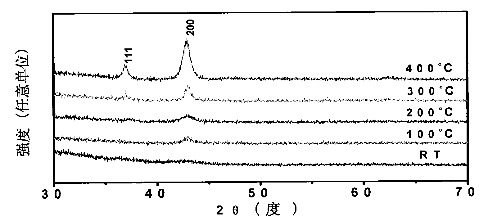
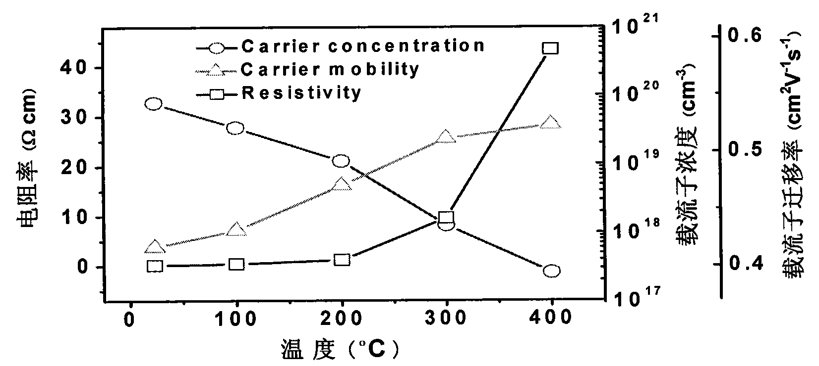
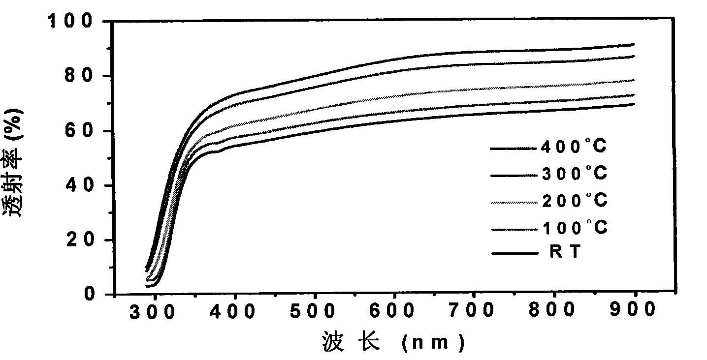
[0017] According to stoichiometric ratio Ni 0.9 Cu 0.1 O Prepare a circular ceramic target with a diameter of 23.4mm. Film preparation by PPD: the substrate is a common glass slide, which has been ultrasonically cleaned by deionized water, acetone and alcohol for 20 minutes each; the distance between the target surface and the quartz tube is fixed at 4mm, and the distance between the target surface and the substrate is 25mm; the substrate temperature changes The range is from room temperature to 400°C; set O 2 For the working air pressure, use Bronkhorst’s mass flowmeter to control its flow, so that the working air pressure is 3.0Pa; the HCL 140-20000 high-voltage DC power output source sets the working voltage and current to -18.0kV and 3.0mA respectively; the pulsed electron beam The frequency is 2.0 Hz; the film deposition time is about 45 minutes.

[0018] The experimental results are shown in the attached figure, figure 2 In, Ni prepared at room temperature 0.9 Cu ...


PUM


Abstract

The invention belongs to the field of transparent electronics study and in particular relates to a p-type conductive transparent copper-doped nickel oxide film and a preparation method thereof. The invention provides a p-type conductive transparent oxide semiconductor film, wherein the film is a copper-doped nickel oxide film with chemical formula being Ni1-xCuxO; and x is more than 0 and not more than 0.3. The preparation method is characterized by taking the common glass as the substrate and utilizing the Ni1-xCuxO ceramic target to prepare the film through the pulsed plasma deposition technology under the conditions of proper substrate temperature, oxygen pressure, pulse current and pulse voltage. The prepared film has such excellent photoelectric properties as high conductivity, high transmissivity in the visible light range and the like. Meanwhile, the preparation method has the advantages of simpleness and convenience in operation and relatively low equipment price. Therefore, the novel film material and the preparation method have certain application potentials in the field of semiconductor optoelectronics.

Description

technical field [0001] The invention belongs to the research field of transparent electronics, and in particular relates to a p-type conductive transparent copper-doped nickel oxide film and a preparation method thereof. Background technique [0002] So far, the transparent oxide semiconductor (TransparentOxideSemiconductor, TOS) materials with continuously improved performance are all n-type semiconductors, and the corresponding p-type materials have not made significant progress, so it is impossible to synthesize high-quality transparent oxide pn Junction, which limits the application of TOS materials in the field of semiconductor optoelectronic devices. The p-type transparent oxide semiconductor has become the bottleneck material for the development of transparent electronics, and further research is needed in terms of material selection, conduction mechanism and synthesis process. [0003] NiO is a wide bandgap p-type semiconductor material, and its conductivity at room...

Claims


Application Information

Patent Timeline
IPC IPC(8): H01B5/14H01B1/02H01B1/08C23C14/22C23C14/08
Inventor 杨铭张群施展
Owner FUDAN UNIV
Why Eureka
Try Eureka