Three-laminated-layer thin film solar cell and preparation method thereof

A solar thin film and triple junction stacking technology, applied in the field of solar cells, can solve the problems such as the inability of solar thin film cells to achieve broad-spectrum absorption, the easy generation of S-W effect by amorphous silicon, and the reduction of the efficiency of solar thin film cells, so as to improve the photoelectric conversion efficiency. , the effect of increasing the band gap width and expanding the spectral absorption range

Active Publication Date: 2011-07-06
BOE TECH GRP CO LTD +1
View PDF0 Cites 4 Cited by
  • Summary
  • Abstract
  • Description
  • Claims
  • Application Information

AI Technical Summary

Problems solved by technology

[0009] However, the inventor found the following defects in the prior art during the research of the present invention: when the traditional amorphous silicon is used as the intrinsic layer of the top cell, since its bandgap width is only 1.7 eV, the wavelength of light absorbed mainly Concentrated at 400-800nm, very little absorption of light with a wavelength of less than 400nm, so that solar thin-film cells cannot achieve broad-spectrum absorption, and at the same time, amorphous silicon is prone to produce S-W effects, thereby reducing the efficiency of solar thin-film cells

Method used


Image

  • Three-laminated-layer thin film solar cell and preparation method thereof
  • Three-laminated-layer thin film solar cell and preparation method thereof
  • Three-laminated-layer thin film solar cell and preparation method thereof

Examples


Embodiment 1

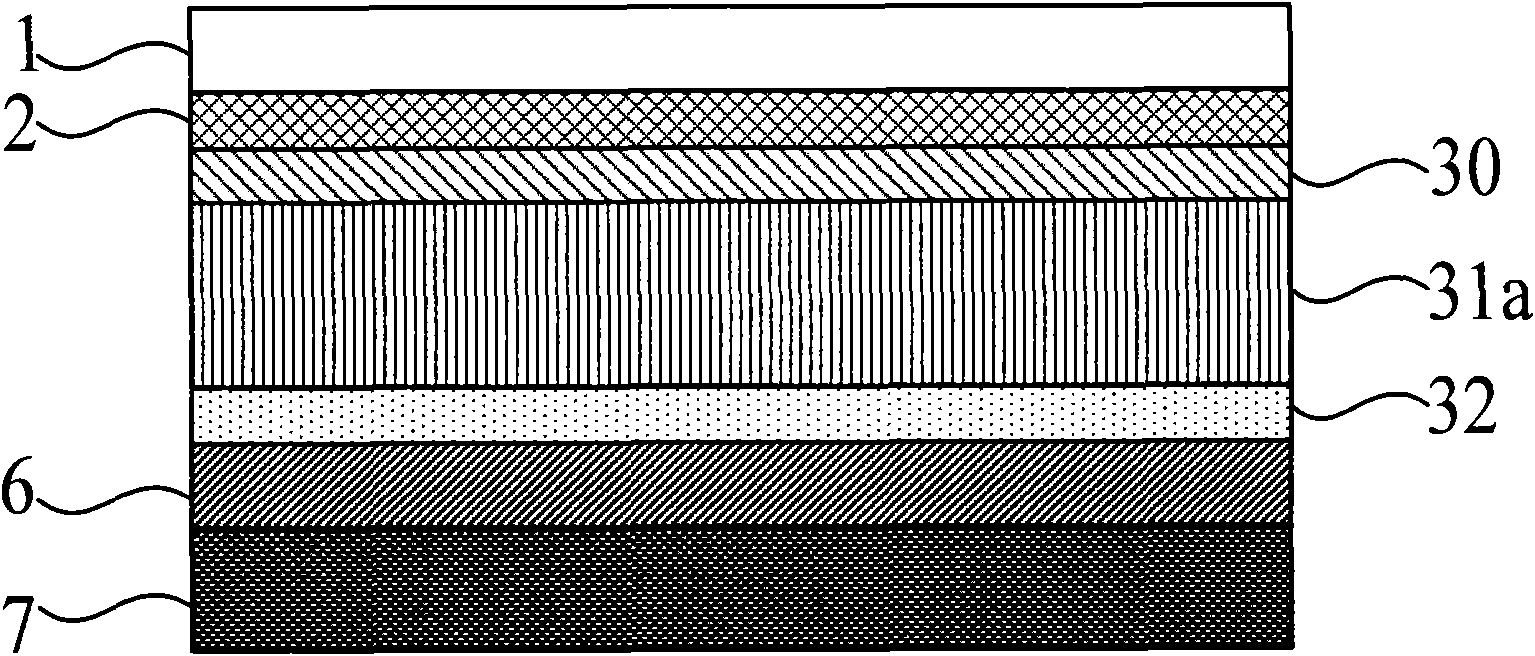
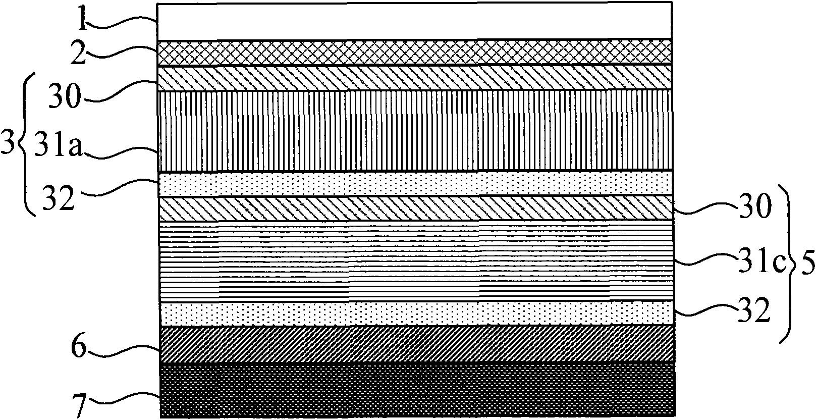
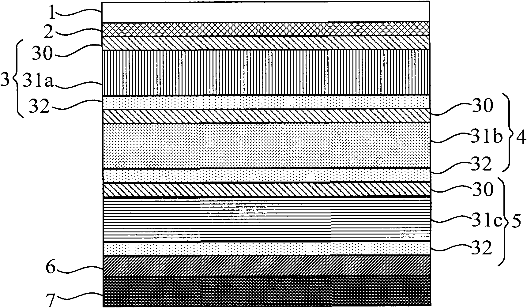
[0036] Figure 4 The structure schematic diagram of the three-junction laminated solar thin film battery provided for Embodiment 1 of the present invention, it can be seen from the figure that the triple-junction laminated solar thin film battery includes a top battery 3, a middle battery 4 and a bottom battery 5, respectively comprising P-type doped layer, intrinsic layer and N-type doped layer, wherein,

[0037] The intrinsic layer of the top cell 3 is an intrinsic nano-silicon film 31d with a grain size of 2-10 nanometers (nm) and a crystallization rate of 10-20%.

[0038] In the present invention, nano-silicon with a grain size of 2-10nm and a crystallization rate of 10-20% is used as the intrinsic layer of the top cell 3, that is, the intrinsic nano-silicon thin film 31d. Therefore, the bandgap width of the top battery 3 is increased to 1.8-2.0ev, so that the solar thin film battery can fully absorb the spectrum with a wavelength less than 400nm, and at the same time, be...

Embodiment 2

[0047] This embodiment provides a method for preparing a triple-junction stacked solar thin film cell, which includes the process of sequentially forming a transparent conductive film, a top cell, an intermediate cell, a bottom cell, a back reflection electrode and a metal back electrode on a transparent substrate. Figure 5 The flow chart of forming the top cell in the preparation method of the triple-junction laminated solar thin film cell provided in Example 2 of the present invention, from Figure 5 As can be seen in the figure, the process of forming the top cell includes:

[0048] Step 100, depositing a boron-doped amorphous silicon carbon layer on the transparent conductive film;

[0049] Step 200, on the boron-doped amorphous silicon carbon layer, using a mixed gas of silane and hydrogen with a silane concentration of 1-5%, at a deposition pressure of 1.0-1.5 Torr (Torr), a deposition temperature of 180-220° C. and Under the glow power of 15-30W, the intrinsic nano-si...


PUM


Abstract

The invention relates to a three-laminated-layer thin film solar cell and a preparation method thereof, wherein the three-laminated-layer thin film solar cell comprises a top cell, a middle cell and a bottom cell, wherein each cell comprises a P-type doping layer, an intrinsic layer and an N-type doping layer, and the intrinsic layer of the top cell is an intrinsic nano-silicon film, wherein the crystallite dimension is 2 to 10 nanometers and the crystallization rate is 10 to 20 percent. In the preparation method of the three-laminated-layer thin film solar cell, the intrinsic nano-silicon film is deposited on a boron-doped amorphous silicon carbon layer with a silane-hydrogen mixed gas under the deposition gas pressure of 1.0 to 1.5 Torr at the deposition temperature of 180 to 220 DEG C with the glow power of 15 to 30 watts when the intrinsic layer of the top cell is formed, wherein the silane concentration of the silane is 1 to 5 percent. The three-laminated-layer thin film solar cell and the preparation method thereof can improve the band gap width of the top cell, enlarge the spectrum absorption range of the thin film solar cell, and overcome S-W effect, thus improving the photoelectric conversion efficiency.

Description

technical field [0001] The invention relates to a solar battery technology, in particular to a triple-junction stacked solar thin film battery and a preparation method thereof. Background technique [0002] At present, with the shortage of energy supply, solar cells that directly convert solar energy into electrical energy have attracted more and more attention. [0003] Commonly used solar cells generally include monocrystalline silicon solar cells, polycrystalline silicon solar cells, amorphous silicon solar cells, and multi-component solar cells according to material classification. Among them, compared with monocrystalline silicon and polycrystalline silicon solar cells, the manufacturing process of amorphous silicon solar cells is greatly simplified, the consumption of silicon materials is small, the power consumption is lower, and it can also generate electricity under weak light conditions. [0004] figure 1 It is a structural schematic diagram of an amorphous silic...

Claims


Application Information

Patent Timeline
Patent Type & Authority Applications(China)
IPC IPC(8): H01L31/075H01L31/20H01L31/076
CPCY02E10/50Y02E10/548Y02P70/50
Inventor 李贵君韩晓艳宋行宾
Owner BOE TECH GRP CO LTD
Why Eureka
Try Eureka