Method for preparing silicon nanowire array with smooth surface

A silicon nanowire array and smooth surface technology, applied in nanotechnology, chemical instruments and methods, silicon compounds, etc., to achieve low-cost effects

Inactive Publication Date: 2011-07-20
SHANGHAI JIAO TONG UNIV
View PDF1 Cites 56 Cited by
  • Summary
  • Abstract
  • Description
  • Claims
  • Application Information

AI Technical Summary

Problems solved by technology

[0004] The present invention aims at the above-mentioned deficiencies in the prior art, and provides a method for preparing silicon nanowire arrays with a controllable length and a smooth surface. By simply adjusting the concentration of the oxidant hydrogen peroxide and the

Method used


Image

  • Method for preparing silicon nanowire array with smooth surface
  • Method for preparing silicon nanowire array with smooth surface
  • Method for preparing silicon nanowire array with smooth surface

Examples


Embodiment 1

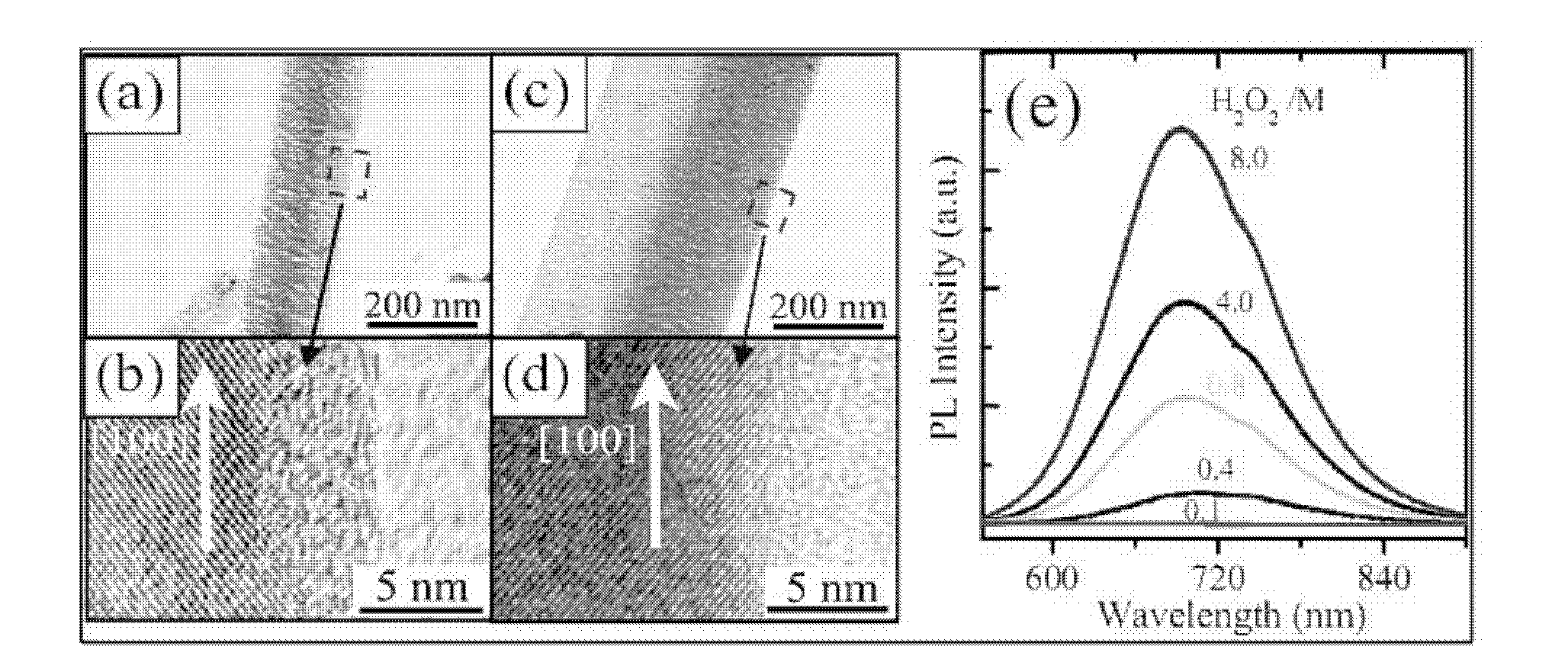
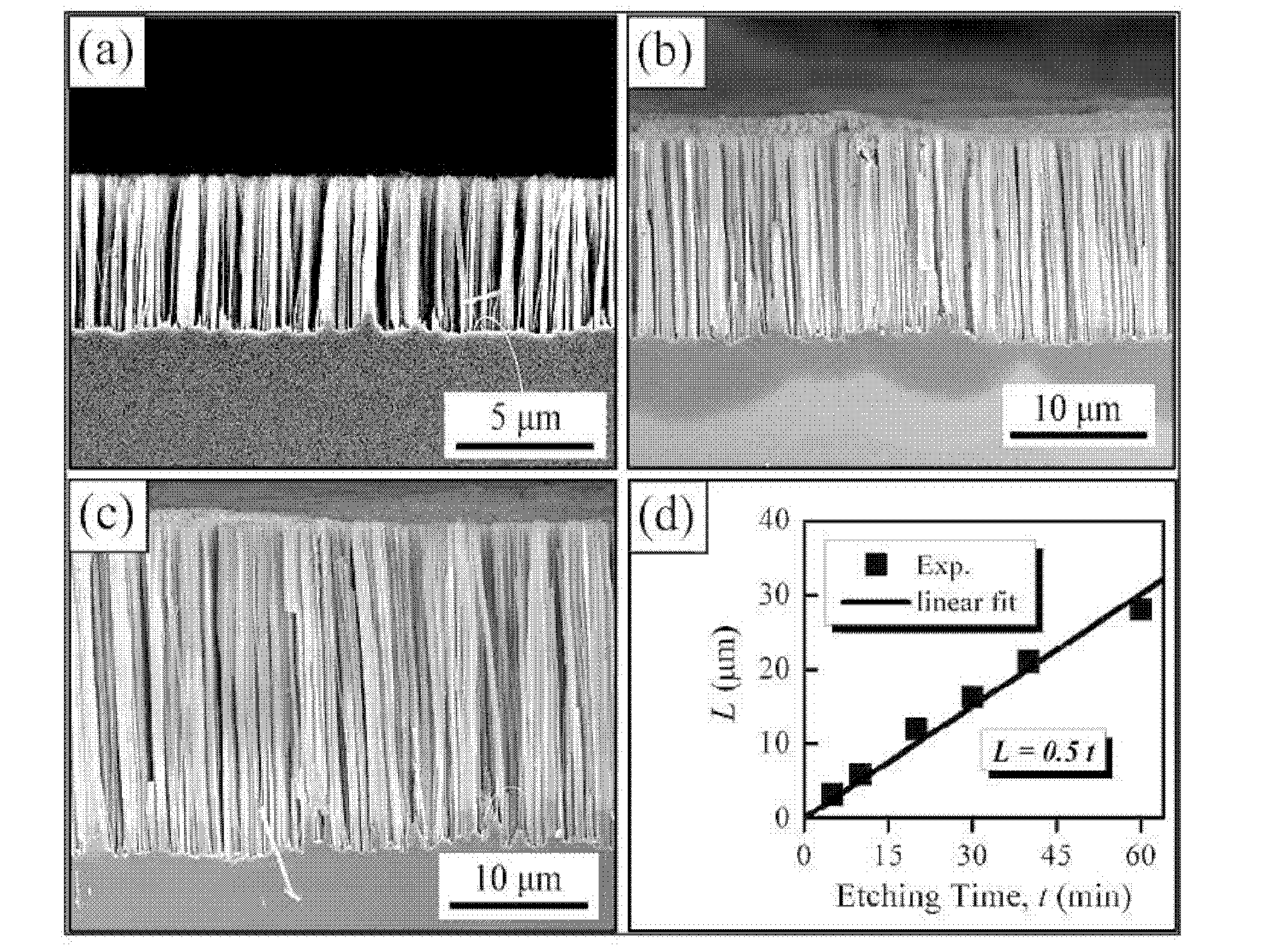
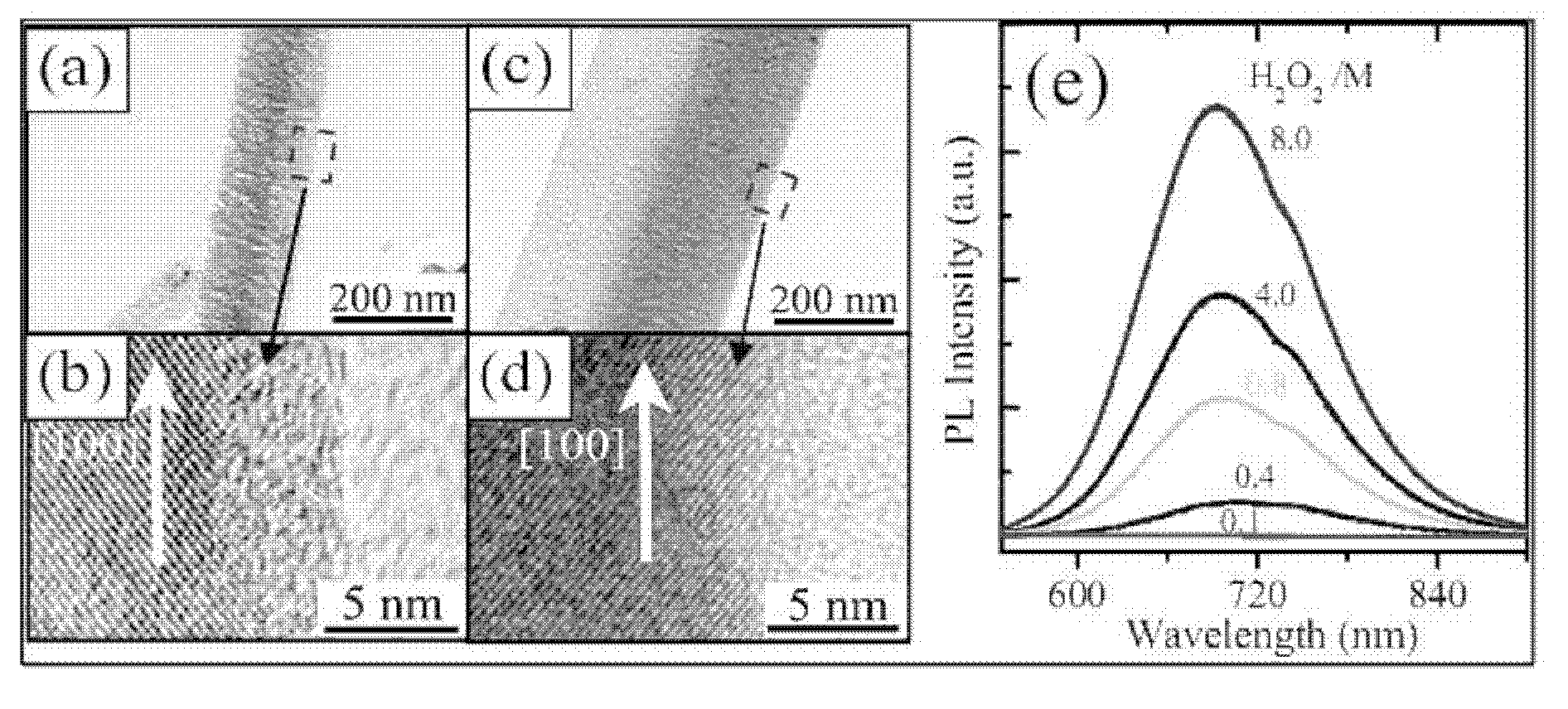
[0018] Using a p-type (100) crystal-oriented electronic-grade silicon wafer with a resistivity of 0.01-0.03Ω·cm, by depositing silver nanoparticles, and then etching them in hydrofluoric acid mixed aqueous solutions at different concentrations of hydrogen peroxide at room temperature; After the etching, the silicon wafers were rinsed with nitric acid and deionized water, dried and then characterized by high-resolution transmission electron microscopy (mainly to study the surface conditions of silicon nanowires). Mann / luminescence spectrometer for photoluminescence test, the excitation light is Ar with a wavelength of 514.5 nm + laser. The specific implementation steps are as follows:

[0019] (1) Silicon wafers were first ultrasonically cleaned with acetone, absolute ethanol, and deionized water for 15 minutes each, and then boiled at 85°C for 15 minutes with ammonia water: hydrogen peroxide: water at a volume ratio of 1:1:5, and then Soak in hydrofluoric acid with a mass fr...

Embodiment 2

[0026] (1) Silicon wafers were first ultrasonically cleaned with acetone, absolute ethanol, and deionized water for 15 minutes each, and then boiled at 85°C for 15 minutes with ammonia water: hydrogen peroxide: water at a volume ratio of 1:1:5, and then Soak in hydrofluoric acid with a mass fraction of 3% for 1 minute to remove the silicon oxide layer; then use hydrochloric acid:hydrogen peroxide:water with a volume ratio of 1:1:5, cook at 85°C for 15 minutes, and finally deionized water Rinse with dilute hydrofluoric acid solution to obtain fluorine-terminated surface-hydrophobic silicon wafers.

[0027] (2) Put the cleaned silicon chip into an aqueous solution with a concentration of 4.0 mol / liter hydrofluoric acid and 10.0 mmol / liter silver nitrate at room temperature, extend the immersion time to 100 seconds, and then take it out quickly, and the surface of the silicon chip is uniform A layer of silver nanoparticles was deposited.

[0028] (3) the silicon chip that deposi...

Embodiment 3

[0033] (1) Silicon wafers were first ultrasonically cleaned with acetone, absolute ethanol, and deionized water for 15 minutes each, and then boiled at 85°C for 15 minutes with ammonia water: hydrogen peroxide: water at a volume ratio of 1:1:5, and then Soak in hydrofluoric acid with a mass fraction of 3% for 1 minute to remove the silicon oxide layer; then use hydrochloric acid:hydrogen peroxide:water with a volume ratio of 1:1:5, cook at 85°C for 15 minutes, and finally deionized water Rinse with dilute hydrofluoric acid solution to obtain fluorine-terminated surface-hydrophobic silicon wafers.

[0034] (2) Put the cleaned silicon chip into an aqueous solution with a concentration of 4.0 mol / liter hydrofluoric acid and 20.0 mmol / liter silver nitrate at room temperature, and the immersion time is 60 seconds, then take it out quickly, and the surface of the silicon chip is evenly deposited layer of silver nanoparticles.

[0035] (3) the silicon chip of depositing the silver n...


PUM

PropertyMeasurementUnit
Resistivityaaaaaaaaaa

Abstract

The invention relates to a method for preparing a length-controlled silicon nanowire array with a smooth surface, and belongs to the technology of the preparation of nanometer materials. The method comprises the following steps of: firstly, performing wet chemical cleaning on a silicon wafer; secondly, depositing a silver nanometer granular layer on the surface of the silicon wafer in mixed solution containing hydrofluoric acid and silver nitrate by an electroless chemical deposition method; thirdly, performing chemical etching by mixed solution containing the hydrofluoric acid and hydrogen peroxide; and finally, removing silver nanometer granules by using nitric acid to obtain the silicon nanowire array. In the method, length-controlled silicon nanowires with the smooth surfaces are prepared by regulating the concentration and etching time of the hydrogen peroxide serving as an oxidant simply in a chemical etch system, so the technical problem of preparing the silicon nanowires with fewer surface defects in metal-assisted chemical etching is solved.

Description

technical field [0001] The invention relates to a method in the technical field of nanomaterial preparation, in particular to a method for preparing a silicon nanowire array with a controllable length and a smooth surface. Background technique [0002] At present, the core of large-scale development and utilization of solar photovoltaic power generation is to reduce the production cost of solar cells and improve the photoelectric conversion efficiency of cells. Silicon nanowires can vertically orthogonalize light absorption and carrier separation (that is, light absorption is along the axial direction of silicon nanowires and carriers are separated in the radial direction of nanowires), compared with traditional flat silicon cells It not only enhances the light absorption but also improves the collection efficiency of carriers, so that it is possible to realize higher efficiency solar cells in silicon materials with shorter carrier diffusion length and low cost. Therefore, ...

Claims


Application Information

Patent Timeline
IPC IPC(8): C01B33/021B82Y40/00
Inventor 沈文忠谢卫强
Owner SHANGHAI JIAO TONG UNIV
Why Eureka
Try Eureka