Capacitor touch pad based on carbon nanotube film
A carbon nanotube film and technology of carbon nanotubes, applied in the direction of electrical digital data processing, input/output process of data processing, instruments, etc., can solve the problem of high cost of capacitive touch panel, achieve low power consumption, reduce cost, The effect of reducing production and processing costs
- Summary
- Abstract
- Description
- Claims
- Application Information
AI Technical Summary
Problems solved by technology
Method used
Image

Examples
Embodiment 1
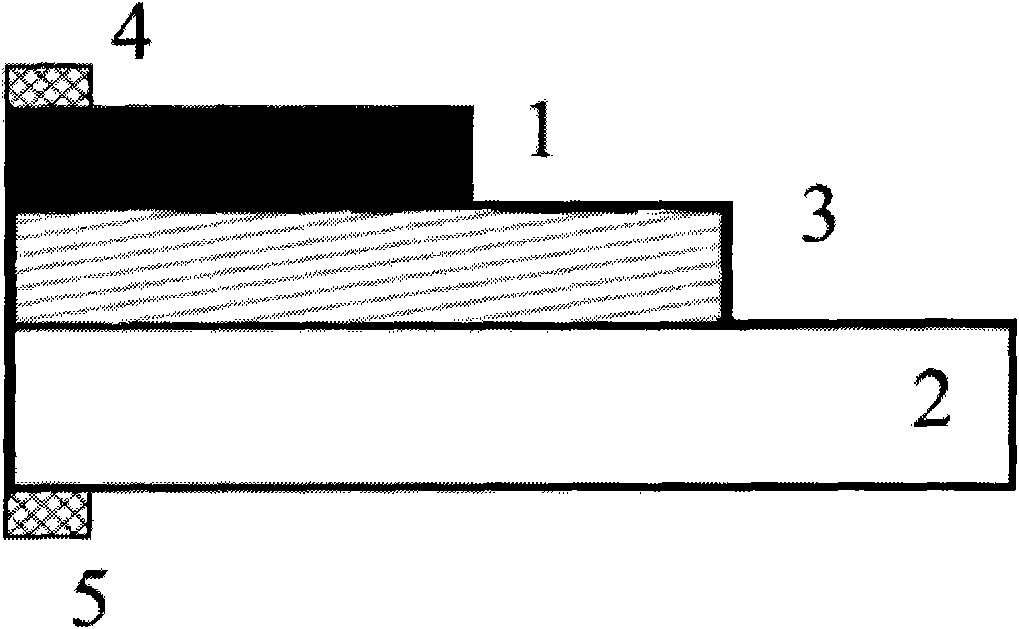
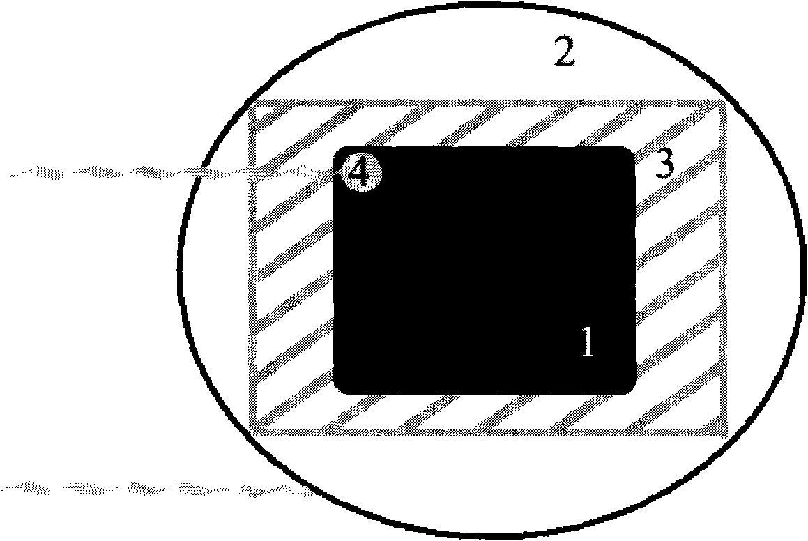
[0046] Embodiment 1 refers to Figure 1-2 , the capacitive touch panel includes a stacked conductive layer 1, a dielectric layer 3 and a conductive base 2, the conductive layer and the conductive base are respectively connected to at least one upper electrode 4 and at least one lower electrode 5, wherein the conductive layer is a carbon nanotube film layer.
[0047] The preparation process of the capacitive touch panel is as follows:
[0048] (1) A carbon nanotube film is selected as the conductive layer 1 .
[0049] (2) Preparation of silicon dioxide substrate: SiO with a thickness of 20 nm is oxidized and evaporated on a highly doped silicon wafer 2 2 Dielectric layer 3.
[0050] (3) Transfer the carbon nanotube film to the silicon dioxide-silicon substrate. Use a copper sheet as an electrode to draw two wires from the carbon nanotube film and the conductive substrate silicon respectively to form a capacitive touch panel.
[0051] The carbon nanotube film involved in thi...
Embodiment 2
[0056] Embodiment 2 The structure of the capacitive touch panel of this embodiment is basically the same as that of Embodiment 1, and its preparation process is as follows:
[0057] (1) select the multi-walled carbon nanotube film as the conductive layer: with reference to Example 1, get the commercially available multi-walled carbon nanotubes to prepare the multi-walled carbon nanotube film as the conductive layer, and the conductivity of the carbon nanotube film is at 30~500Ω / □, the tensile strength is between 200 and 500 MPa.
[0058] (2) Preparation of single-walled carbon nanotube film-polymer substrate: disperse single-walled carbon nanotubes to prepare a single-walled carbon nanotube film, which is attached to the lower end surface of the polymer film as a conductive substrate, and the polymer film as a dielectric Layer, the polymer film can choose polyvinyl alcohol, polyvinyl formal, polyethylene, cellulose and other insulating materials.
[0059] (3) Transfer the pr...
Embodiment 3
[0061] Embodiment 3 The structure of the capacitive touch panel of this embodiment is basically the same as that of Embodiments 1 and 2, and its preparation process is as follows:
[0062] (1) Select a certain mass ratio of single-wall and multi-wall carbon nanotube mixed films as the conductive layer: with reference to Example 1, get commercially available single-wall carbon nanotubes and multi-wall carbon nanotube mixed powders to prepare mixed carbon nanotubes The thin film acts as a conductive layer.
[0063] (2) Preparation of mica-aluminum substrate: A mica sheet with a thickness of about tens of microns is attached to the metal aluminum film, the aluminum film is used as a conductive substrate, and the mica sheet is used as a dielectric layer.
[0064] (3) The prepared mixed carbon nanotube film was transferred to the mica-aluminum substrate, and copper sheets were used as electrodes to draw two wires from the mixed carbon nanotube film and the metal aluminum film respe...
PUM
| Property | Measurement | Unit |
|---|---|---|
| Tensile strength | aaaaa | aaaaa |
| Thickness | aaaaa | aaaaa |
| Thickness | aaaaa | aaaaa |
Abstract
Description
Claims
Application Information
 - R&D
- Intellectual Property
- Life Sciences
- Materials
- Tech Scout
- Unparalleled Data Quality
- Higher Quality Content
- 60% Fewer Hallucinations
Browse by: Latest US Patents, China's latest patents, Technical Efficacy Thesaurus, Application Domain, Technology Topic, Popular Technical Reports.
© 2025 PatSnap. All rights reserved.Legal|Privacy policy|Modern Slavery Act Transparency Statement|Sitemap|About US| Contact US: help@patsnap.com