Silicon-on-insulator N-type transverse insulated gate bipolar transistor and preparation method thereof

A bipolar transistor and silicon-on-insulator technology, which is applied in the manufacture of semiconductor/solid-state devices, semiconductor devices, electrical components, etc., can solve the problems of reducing the current capability of the device, affecting the impurity concentration of the P-type doped body region, etc., to improve triggering. Effects of Threshold Conditions

Inactive Publication Date: 2012-09-19
SOUTHEAST UNIV
View PDF0 Cites 0 Cited by
  • Summary
  • Abstract
  • Description
  • Claims
  • Application Information

AI Technical Summary

Problems solved by technology

However, the formation of a deep P well often affects the impurity concentration of the P-type doped body region, which will increase the threshold voltage of the device and reduce the current capability of the device.

Method used


Image

  • Silicon-on-insulator N-type transverse insulated gate bipolar transistor and preparation method thereof
  • Silicon-on-insulator N-type transverse insulated gate bipolar transistor and preparation method thereof
  • Silicon-on-insulator N-type transverse insulated gate bipolar transistor and preparation method thereof

Examples


Embodiment Construction

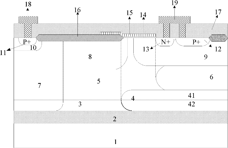
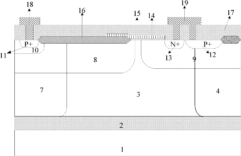
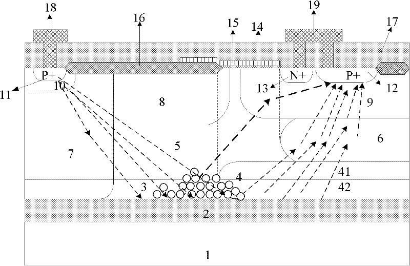
[0025] refer to figure 1, a silicon-on-insulator N-type lateral insulated gate bipolar transistor, comprising: a P-type substrate 1, a buried oxide layer 2 is arranged on the P-type substrate 1, and a first P-type oxide layer is arranged on the buried oxide layer 2 The epitaxial layer 3 is provided with a second P-type epitaxial layer 5 above the first P-type epitaxial layer 3, and an N-type doped deep well 7 is provided on the left side of the second P-type epitaxial layer 5. An N-type doped drift region 8 is arranged in the well 7 and part of the second P-type epitaxial layer 5, and an N-type buffer layer 10 is arranged in the N-type doped drift region 8, and a P-type buffer layer 10 is arranged in the N-type buffer layer 10. The doped anode contact region 11 is provided with a P-type doped channel region 9 on the right side of the second P-type epitaxial layer 5, and an N-type doped cathode contact region 13 and The P-type doped body contact region 12 is provided with a f...


PUM


Abstract

The invention relates to a silicon-on-insulator N-type transverse insulated gate bipolar transistor and a preparation method thereof. The silicon-on-insulator N-type transverse insulated gate bipolar transistor comprises a P-type silicon-on-insulator silicon wafer, wherein the right region of a first P-type epitaxial layer is provided with a P-type buried layer; a second P-type epitaxial layer isarranged above the first P-type epitaxial layer; a P-type high-energy ion-implantation layer and a P-type channel region are arranged in the second P-type epitaxial layer; the left side is provided with an N-type deep well and an N-type drift region; an N-type buffer layer and a P-type anode contact region are arranged in the N-type drift region; an N-type cathode contact region and a P-type bodycontact region are arranged in the P-type channel region; a first field oxide layer and a gate oxide layer are arranged above the N-type drift region; the gate oxide layer extends rightwards to abovethe P-type channel region; and polycrystalline silicon is arranged above the gate oxide layer and used as a gate. The preparation method comprises the following steps: carrying out implantation onto the right region of the first P-type epitaxial layer to form the P-type buried layer, and carrying out implantation onto the right region of the second P-type epitaxial layer to form the P-type high-energy ion-implantation layer which is communicated with the P-type buried layer, so that the concentration gradually increases from bottom to top so as to form an electrically conductive path which can effectively inhibit the latch effect.

Description

technical field [0001] The invention relates to the field of high-voltage power semiconductor devices, and more precisely, relates to a silicon-on-insulator N-type lateral insulated gate bipolar transistor with suppressed latch-up effect suitable for high-voltage and high-power application conditions and a preparation method thereof. Background technique [0002] With the increasing demand for modern life, the performance of power integrated circuits has attracted more and more attention. Among them, the ability of power integrated circuits to handle high voltage and high current has become one of the most important performance indicators. The factors that determine the ability of power integrated circuits to handle high voltage and high current are not only the circuit structure and design of the power integrated circuit itself, but also the manufacturing process adopted by the circuit. The current capability that a single device with the same area can pass is a measure of t...

Claims


Application Information

Patent Timeline
Patent Type & Authority Patents(China)
IPC IPC(8): H01L29/739H01L29/08H01L21/331H01L21/265
Inventor 时龙兴刘斯扬祝靖朱奎英钱钦松孙伟锋陆生礼
Owner SOUTHEAST UNIV
Why Eureka
Try Eureka