Laminated organic light emitting diode and preparation method thereof
A light-emitting diode and organic technology, applied in organic chemistry, semiconductor/solid-state device manufacturing, electrical components, etc., can solve problems such as increased brightness and current efficiency, increased voltage, and no improvement in the power efficiency of stacked organic light-emitting diodes. Increased brightness and current efficiency, reduced operating voltage, and improved power efficiency
- Summary
- Abstract
- Description
- Claims
- Application Information
AI Technical Summary
Problems solved by technology
Method used
Image

Examples
preparation example Construction
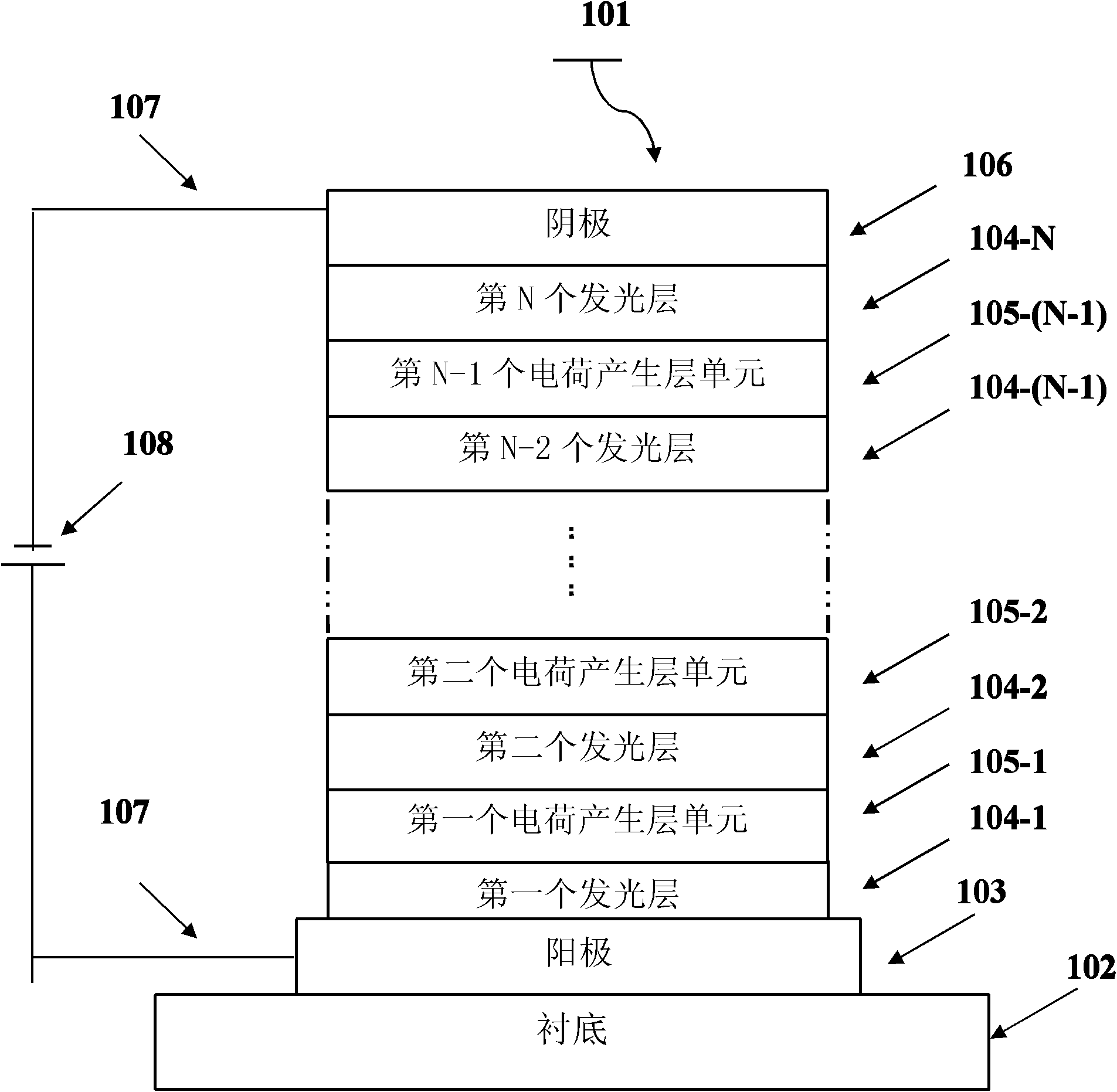
[0042] The invention also discloses a method for preparing a laminated organic light emitting diode, comprising:
[0043] evaporating at least two light-emitting layers between the anode and the cathode;
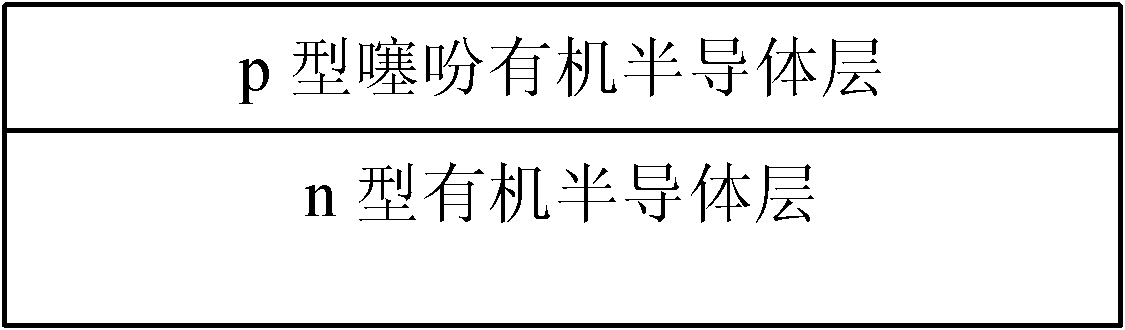
[0044] A charge generation layer is vapor-deposited between adjacent light-emitting layers, the charge generation layer is a heterojunction formed by an n-type organic semiconductor and a p-type organic semiconductor, the p-type organic semiconductor is a thiophene compound, and the p-type organic semiconductor The highest occupied molecular orbital energy level of the semiconductor is less than 6eV, and the difference between the highest occupied molecular orbital energy level of the p-type organic semiconductor and the lowest unoccupied molecular orbital energy level of the n-type organic semiconductor is less than 1eV.
[0045] The substrate is preferably a glass substrate or a flexible substrate, and the flexible substrate is preferably a polycarbonate flexible substrate...
Embodiment 1
[0053] The anode layer ITO on the ITO glass is photolithographically formed into thin strip electrodes, then cleaned, dried with nitrogen, treated with oxygen plasma for 2 minutes, and then transferred to the vacuum coating system;
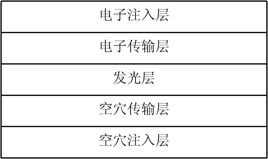
[0054] Wait until the vacuum degree in the vacuum coating system reaches 5×10 -4 4.5 nm MoO was sequentially deposited on the ITO electrode 3 Hole injection layer, 90nm NPB hole transport layer, 30nm C545T doped in Alq 3 Light-emitting layer composed of medium, 30nm Alq 3 Electron transport layer, 1nm LiF electron injection layer, 20nm C 60 n-type organic semiconductor, 10nm NaT3p-type organic semiconductor, 3nm MoO 3 Hole injection layer, 50nm NPB hole transport layer, 30nm C545T doped in Alq 3 Light-emitting layer composed of medium, 30nm Alq 3 An electron transport layer, an electron injection layer of 1 nanometer LiF, and a metal cathode Al of 120 nanometers, wherein the positive and negative electrodes intersect each other to form a ligh...
Embodiment 2
[0057] The anode layer ITO on the ITO glass is photolithographically formed into thin strip electrodes, then cleaned, dried with nitrogen, treated with oxygen plasma for 2 minutes, and then transferred to the vacuum coating system;
[0058] Wait until the vacuum degree in the vacuum coating system reaches 5×10 -4 4.5 nm MoO was sequentially deposited on the ITO electrode 3 Hole injection layer, 120nm NPB hole transport layer, 30nm C545T doped in Alq 3 Light-emitting layer composed of medium, 30nm Alq 3 Electron transport layer, 1nm LiF electron injection layer, 20nm C 60 n-type organic semiconductor, 10nm TNT2p-type organic semiconductor, 3nm MoO 3 Hole injection layer, 50nm NPB hole transport layer, 30nm C545T doped in Alq 3 Light-emitting layer composed of medium, 30nm Alq 3 An electron transport layer, an electron injection layer of 1 nanometer LiF, and a metal cathode Al of 120 nanometers, wherein the intersecting parts of the positive and negative electrodes form a l...
PUM
| Property | Measurement | Unit |
|---|---|---|
| Thickness | aaaaa | aaaaa |
| Thickness | aaaaa | aaaaa |
| Thickness | aaaaa | aaaaa |
Abstract
Description
Claims
Application Information
 - Generate Ideas
- Intellectual Property
- Life Sciences
- Materials
- Tech Scout
- Unparalleled Data Quality
- Higher Quality Content
- 60% Fewer Hallucinations
Browse by: Latest US Patents, China's latest patents, Technical Efficacy Thesaurus, Application Domain, Technology Topic, Popular Technical Reports.
© 2025 PatSnap. All rights reserved.Legal|Privacy policy|Modern Slavery Act Transparency Statement|Sitemap|About US| Contact US: help@patsnap.com