NAND Flash-based data recording method and recording controller

A data recording and controller technology, applied in the direction of input/output to record carrier, memory address/allocation/relocation, etc., can solve problems such as rewriting, writing bandwidth is difficult to continue to improve, and heat generation is large

Inactive Publication Date: 2011-08-31
INST OF OPTICS & ELECTRONICS - CHINESE ACAD OF SCI
View PDF5 Cites 68 Cited by
  • Summary
  • Abstract
  • Description
  • Claims
  • Application Information

AI Technical Summary

Problems solved by technology

[0005] 2. Unstable
The mechanical structure of the hard disk leads to a high failure rate of the hard disk
Wear of the magnetic head, deformation of the cantilever, and slight deformation of the hard disk casing, disk surface or motor after the hard disk is subjected to vibration will lead to unstable performance of the hard disk
At present, ordinary hard disks can only withstand an impact of about 100 g in a non-working state, so traditional hard disks are not suitable for complex conditions such as mobile facilities or places with large vibrations.
Especially in practical applications, the shaking of the equipment will seriously affect the stability of the rotation of the mechanical hard disk, which will greatly reduce the reliability of data collection.
[0006] 3. High power consumption and high heat generation
[0015] 1. ROM has the characteristics of high density, high reliability, and data non-loss, but its content cannot be changed after leaving the factory, so it cannot be used as a storage medium for recorders at all
[0016] 2. EPROM has the characteristics of data non-loss, high density, rewritable, etc., but it cannot be rewritten when the system is online. It must be removed from the system and erased with ultraviolet light before rewriting, so it cannot be used with a recorder. storage medium
[0017] 3. EERPOM is data non-losing and supports online rewriting of the system, but because high voltage pulses are required for erasing and writing, and the time for erasing and writing is long, EERPOM is still in the normal working state of the system. Can only work in the read state
[0018] 4. The most basic storage unit of DRAM is a CMOS transistor, which is driven by a capacitor and stores data by charging and discharging. Its advantages lie in its high density and fast access speed, but its data loss requires continuous The power supply (power loss and data loss), and needs to be supplemented by the necessary refresh control circuit, so it consumes more power
[0019] 5. The storage unit of SRAM is actually a flip-flop. The data can be kept without power-off and does not need to be refreshed. Its power consumption is lower than that of DRAM and its speed is faster. However, the storage density of SRAM is very low. So now SRAM is mostly used in small storage capacity systems (also belongs to memory that loses data after power failure)
[0026] 3. The transmission efficiency is very high, and it is very cost-effective in the small capacity of 1-4MB, but the lower writing and erasing speed greatly affects its performance
[0033] 5. The chip contains an invalid block
This increases the complexity of the system control
[0038] 3. Due to manufacturing process and cost reasons, any manufacturer's NAND flash contains bad blocks (ie invalid blocks, invalid blocks) when they leave the factory, and the number of bad blocks will increase during use
[0047] 1. Unable to switch between embedded applications and non-embedded applications, poor adaptability and flexibility
[0048] 2. There is no simple and effective wear leveling at the bottom of the hardware, and the life of the recorder is affected
[0049] 3. It does not have NAND Flash cross-writing and cross-parallel writing control functions, and can only use multiple groups of NAND Flash for inter-group pipeline operations. In the case of certain FPGA pin resources, the recording parallelism will be affected, and the writing bandwidth will be affected. hard to keep improving

Method used


Image

  • NAND Flash-based data recording method and recording controller
  • NAND Flash-based data recording method and recording controller
  • NAND Flash-based data recording method and recording controller

Examples


Embodiment 1

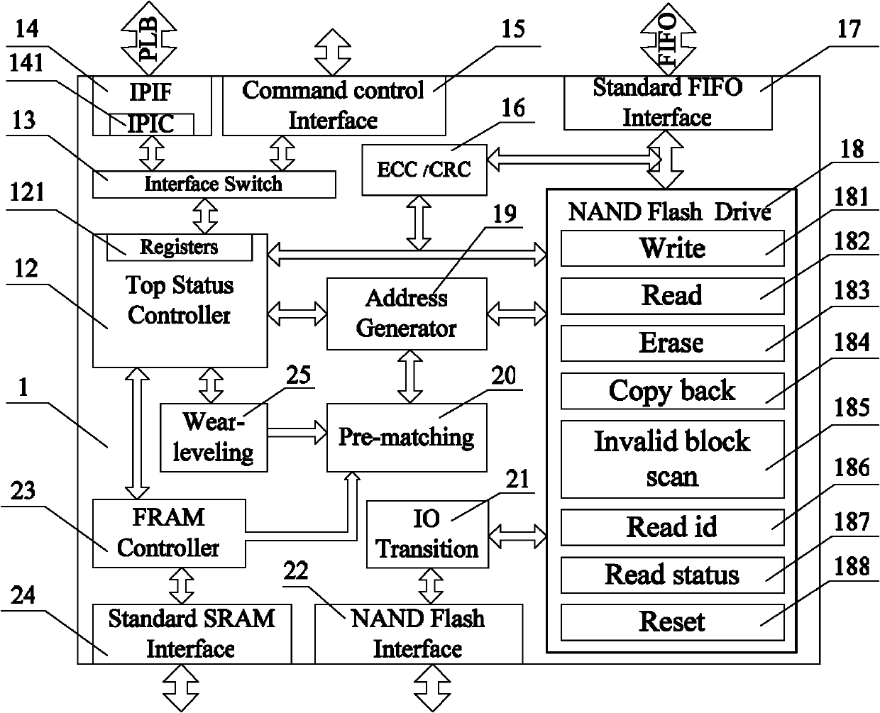
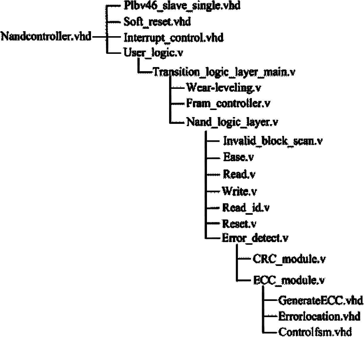
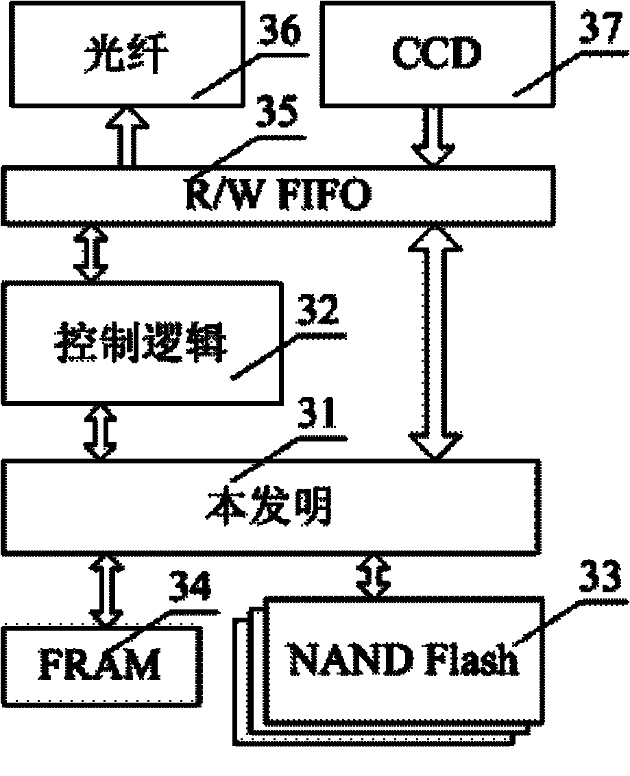
[0158] This example takes a non-embedded application as an example. The image data of the CCD camera is recorded in the NAND Flash array, and the recorded data is read out through the optical fiber interface, and then the erase operation is performed. The technical scenario is: the system connects 42 Samsung K9WBG08U1MSLC NAND flash chips in parallel, each 4GB, including 16384 blocks, each block has 64 pages, and each page (4K+128)B. The total system capacity is 168GB, the reserved capacity for bad block management is 8GB, and the effective image storage capacity of the system is 160GB. The FRAM uses Ramtron's FM20L08 ferroelectric memory with a capacity of 128KB. FPGA adopts Xilinx VIRTEX-5 XC5VFX70T chip. The image comes from a Pantera SA 2M30 high-definition CCD camera with a frame rate of 120frame / s, a resolution of 1600×1200pixels, and a grayscale of 10bits. Peripheral modules in the example are designed with Verilog hardware language.

[0159] Attached below image 3...

Embodiment 2

[0187] In this embodiment, the present invention is applied in an embedded design to record the image data of a CCD camera in a NAND Flash array, and read out the recorded data through a Gigabit network. The technical scenario is: the system uses 42 Samsung K9WBG08U1M SLCNAND flash chips connected in parallel, each 4GB, including 16384 blocks, each block 64 pages, each page (4K+128)B. The total system capacity is 168GB, the reserved capacity for bad block management is 8GB, and the effective image storage capacity of the system is 160GB. The FRAM uses Ramtron's FM20L08 ferroelectric memory with a capacity of 128KB. The image comes from a Pantera SA 2M30 high-definition CCD camera with a frame rate of 120frame / s, a resolution of 1600×1200pixels, and a grayscale of 10bits. FPGA adopts XilinxVIRTEX-5XC5VFX70T chip. The embedded CPU adopts the PPC440 hard core 1,01A version in the FPGA, the working frequency is 400MHz, and the PLB bus working frequency is 100MHz. The memory con...


PUM


Abstract

The invention discloses an NAND Flash-based data recording method and an NAND Flash-based data recording controller. The method comprises the following methods: a hardware bad block management method comprising the following steps of: when a sudden bad block appears, jumping to a next matched valid block without time delay to continuously record, and finally writing the data lag of a page before the bad block appears back to the jumped valid block; a hardware balance method comprising the following step of: starting the erasing-writing operation in succession to the last erasing-writing address so that the erasing-writing times of each block of the NAND Flash is approximately equal; and an input output (IO) expansion method comprising the following steps of: converting data bit width and switching control signals so that a single NAND Flash driver can control multiple chips and multiple groups of NAND Flashes. The controller comprises a ferroelectric random access memory (FRAM) controller, a top state controller, a loss equalizer, an interface switching module, a pre-matching module, an address generating module, a register set, a data verification module, a standard first in first out (FIFO) interface, a standard static random access memory (SRAM) interface, a command control interface and the NAND Flash driver. The whole controller can be mounted on a processor local bus (PLB) of an embedded processor, and data conversion between a control signal and a state signal can be performed through the command control interface and an external module.

Description

technical field [0001] The invention relates to the realization of a NAND Flash data recording controller, especially the realization of a high-speed and high-reliability NAND Flash data recording controller. Large-scale field programmable gate array (Field Programable Gate Array, FPGA) is used as the implementation platform to realize high-speed recording, storage, reading and erasing of data in a single-chip NAND Flash or NAND Flash array without affecting the recording performance. To achieve effective bad block management under certain circumstances. Background technique [0002] Data recording technology has always been one of the key technologies in domestic and foreign research in the fields of aviation, spaceflight, and navigation. In practical applications, it is necessary to record the collected high-speed real-time data (such as high-resolution image data) in real time for post-processing. With the improvement of the accuracy of collected data and the increase o...

Claims


Application Information

Patent Timeline
Patent Type & Authority Applications(China)
IPC IPC(8): G06F12/06G06F3/06
Inventor 任国强徐永刚姚俊张峰李其虎
Owner INST OF OPTICS & ELECTRONICS - CHINESE ACAD OF SCI
Why Eureka
Try Eureka