Back face passivating structure and method for floating junction of solar cell

A solar cell and backside passivation technology, which is applied in the direction of circuits, photovoltaic power generation, electrical components, etc., can solve the problems of reducing series connection, high diffusion temperature, poor optical and electrical performance of aluminum back field, etc., to increase voltage and efficiency, reduce composite effect

Active Publication Date: 2013-09-04
TRINA SOLAR CO LTD
View PDF4 Cites 0 Cited by
  • Summary
  • Abstract
  • Description
  • Claims
  • Application Information

AI Technical Summary

Problems solved by technology

[0003] 1) Al BSF: A layer of 2-20um Al is plated on the back of the solar cell by deposition or screen printing, and an aluminum back field is formed after annealing or sintering, which plays the role of back passivation and improves the current and voltage. , also reduces the series connection, this method is commonly used in mass production, but it will introduce warping of the silicon wafer, especially when the silicon wafer is relatively thin, and the optical and electrical properties of the aluminum back field are relatively poor;
[0004] 2) B diffusion on the back: B is expanded on the back of the p-type silicon wafer to form a P+, but the diffusion temperature is high, the requirements for silicon wafers and equipment are high, and the cost is relatively high;
[0005] 3) LFC is laser sintering electrode: grow or deposit one or more dielectric layers on the back of the silicon wafer, then deposit a layer of aluminum on the dielectric layer, and use laser ablation on the aluminum film to be prepared to make the aluminum penetrate The dielectric layer is integrated into the silicon substrate and forms a good ohmic contact with the silicon substrate, but its cost is high and the process is relatively complicated

Method used


Image

  • Back face passivating structure and method for floating junction of solar cell

Examples


Embodiment Construction

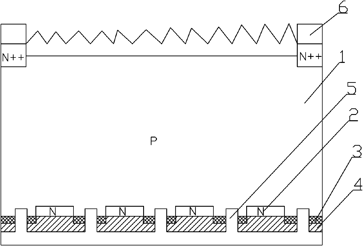
[0021] Such as figure 1 As shown, a solar cell floating junction rear passivation structure, a layer of N-type region 2 is added on the back of P-type silicon substrate 1, and a passivation layer is grown or deposited on the N-type region 2.

[0022] The method for making the passivation structure is as follows: after the silicon chip is cleaned and textured, a layer of 50nm-300nm silicon dioxide film is grown on the surface of the silicon chip by thermal oxidation.

[0023] Grooves are made on the front electrode 6 of the silicon dioxide on the front of the battery for heavy diffusion to form an emitter junction on the front, and the silicon dioxide on the front acts as a diffusion barrier. The silica on the front side is completely removed after the front side re-diffusion is complete.

[0024] The silicon dioxide 3 on the back is reserved, and the reserved thickness is 20-200nm, and then grooves are made in the diffusion N-type region 2 of the silicon dioxide 3 on the back...


PUM


Abstract

The invention relates to the technical field of passivation of solar cells, in particular to a back face passivating method for a floating junction of a solar cell. In the conventional back face passivating route of a P-type crystalline silicon cell, silicon dioxide or silicon nitride is taken as a passivating layer of a back face, a cavity on the back face is a minority carrier, the charge of the arranged passivating layer is positive, and the movement of the cavity to the back face is prevented, so that the back face passivating effect cannot be achieved. In the invention, an N-type region is formed on the back face, so that compounding of the back face is greatly reduced, and the voltage and the efficiency are increased. The structure is as follows: a layer of N-type region is arranged on the back face of a P-type silicon substrate, and a passivation layer is grown or deposited on the N-type region. A process method comprises the following steps of: manufacturing a layer of silicon dioxide film on the surface of a silicon chip after the silicon chip is cleaned and flocked; removing the silicon dioxide on a front face after front face diffusion; grooving and diffusing on the silicon dioxide on the back face; forming an N-type passivating layer on the back face; and depositing passivating films on the front face and the back face respectively.

Description

technical field [0001] The invention relates to the technical field of solar cell passivation, in particular to a method for passivating the back side of a floating junction of a solar cell. Background technique [0002] The preparation method of the traditional solar cell, its process flow is cleaning texturing, diffusion, edge etching and PSG removal, PECVD SiNx film plating, screen printing the Ag electrode on the front and the Al back field and electrode on the back, sintering and electrical properties test. This traditional process determines that the efficiency of the solar cell cannot be greatly improved under the existing process conditions, especially the voltage of the cell must be greatly increased. Among the light absorbed by silicon, most of the light reaches the silicon substrate and the back surface. The high recombination rate in these places is the main factor limiting the improvement of solar cell efficiency. Therefore, many researchers regard the back pas...

Claims


Application Information

Patent Timeline
Patent Type & Authority Patents(China)
IPC IPC(8): H01L31/042H01L31/0352H01L31/18H01L31/0216
CPCH01L31/1868Y02E10/50Y02P70/50
Inventor 邓伟伟冯志强
Owner TRINA SOLAR CO LTD
Why Eureka
Try Eureka