

Method for purifying polycrystalline silicon by directional solidification and slag refining
A directional solidification, refining and purification technology, applied in the direction of self-solidification, polycrystalline material growth, chemical instruments and methods, etc., can solve the problems of silicon slag melt disturbance, difficult to meet the requirements of industrialization, and the results are not very ideal. Good effect, effective removal, simple effect
- Summary
- Abstract
- Description
- Claims
- Application Information
AI Technical Summary
Problems solved by technology
Method used
Image

Examples
Embodiment 1
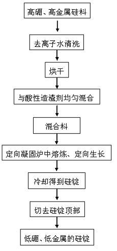
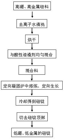
[0020] First, take a polysilicon block with a boron content of 0.001% and a total metal content of 0.05%, wash it with deionized water for 5 times, put it in a drying oven and dry it at 60°C, take 500g of the dried polysilicon block and 500g of acid Slagging agent SiO 2 -CaO-Na 2 CO 3 Mix evenly according to the slag-silicon ratio of 1 to form a mixture, in which the acidic slagging agent SiO 2 -CaO-Na 2 CO 3 The mass percentage of each component is SiO 2 80%, CaO15% and Na 2 CO 3 5%;
[0021] Then slowly pour the mixture into the graphite crucible in the directional solidification furnace, close the furnace cover, turn on the mechanical pump to evacuate to 800Pa, then turn on the Roots pump to evacuate to 3Pa, and open the upper, side and lower three parts of the directional solidification furnace A graphite heating element, and keep the power of the three heating elements the same, start heating up, when the temperature rises to 1200 ° C, flow argon gas protection, h...
Embodiment 2
[0024] First, take a polysilicon block with a boron content of 0.0015% and a total metal content of 0.06%, wash it with deionized water for 5 times, put it in a drying oven and dry it at 60°C, take 500g of the dried polysilicon block and 600g of acid Slagging agent SiO 2 -CaO-Na 2 O is uniformly mixed according to the slag-silicon ratio of 1.2 to form a mixture, in which the acidic slagging agent SiO 2 -CaO-Na 2 The mass percentage of each component of O is SiO 2 60%, CaO25% and Na 2 O15%;
[0025] Then slowly pour the mixture into the graphite crucible in the directional solidification furnace, close the furnace cover, turn on the mechanical pump to evacuate to 800Pa, then turn on the Roots pump to evacuate to 3Pa, and open the upper, side and lower three parts of the directional solidification furnace A graphite heating element, and keep the power of the three heating elements the same, start heating up, when the temperature rises to 1200 ° C, flow argon protection, hea...
PUM
 Abstract
Description
Claims
Application Information