Modulation method for silicon-based GaN crystal structure with optimal field emission performance

A technology of crystal structure and modulation method, which is applied in the field of crystal structure modulation for optimizing the field emission performance of GaN thin films, can solve the problems of few reports on the field emission performance of GaN film cathodes, and improve the field emission performance, shorten the development cycle, and save research and development. cost effect

Inactive Publication Date: 2012-11-21
BEIJING UNIV OF TECH
View PDF0 Cites 0 Cited by
  • Summary
  • Abstract
  • Description
  • Claims
  • Application Information

AI Technical Summary

Problems solved by technology

However, there are very few reports on the field emission performance of GaN thin film cathodes prepared by physical methods.

Method used


Image

  • Modulation method for silicon-based GaN crystal structure with optimal field emission performance
  • Modulation method for silicon-based GaN crystal structure with optimal field emission performance
  • Modulation method for silicon-based GaN crystal structure with optimal field emission performance

Examples


Embodiment 1

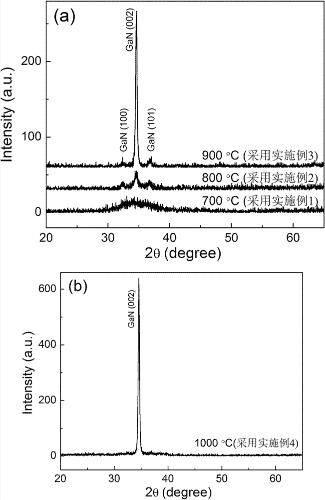
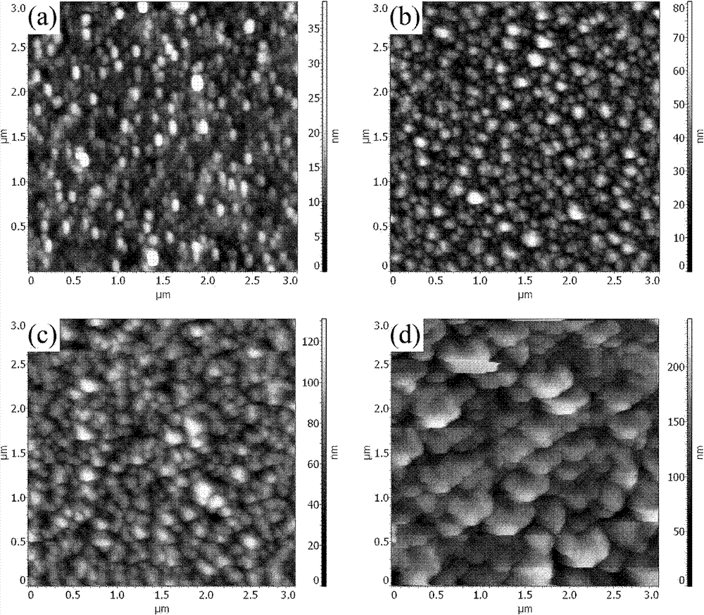
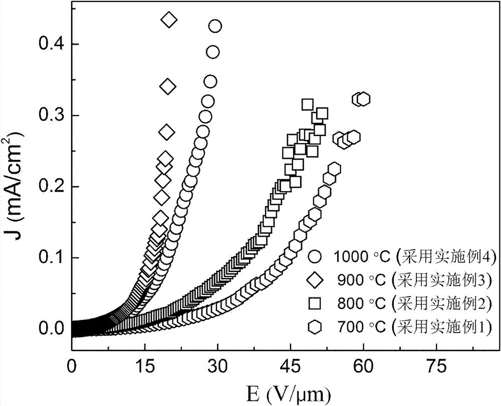
[0025] Using polished n-type (100) silicon as the substrate, gallium nitride powder with a purity of 99.99% was sintered at 560°C for 120 minutes to make a gallium nitride target, and the substrate and target were placed in the cavity of the laser pulse deposition system. The target base distance is 65mm, and the deposition chamber is pumped to about 5×10 -4 Pa, supply nitrogen with a purity of 99.99% as a protective gas and adjust the working pressure of the deposition chamber to 1Pa, set the pulse laser frequency to 10Hz, pulse energy to 350mJ / pulse, heat the substrate to 700°C to obtain low crystallinity by deposition Hexagonal GaN thin films.

Embodiment 2

[0027] Using polished n-type (100) silicon as the substrate, gallium nitride powder with a purity of 99.99% was sintered at 560°C for 120 minutes to make a gallium nitride target, and the substrate and target were placed in the cavity of the laser pulse deposition system. The target base distance is 65mm, and the deposition chamber is pumped to about 5×10 -4 Pa, supply nitrogen with a purity of 99.99% as a protective gas and adjust the working pressure of the deposition chamber to 1Pa, set the pulse laser frequency to 10Hz, pulse energy to 350mJ / pulse, and heat the substrate to 800°C to obtain lower crystallization degree of hexagonal multi-orientation gallium nitride thin film.

Embodiment 3

[0029] Using polished n-type (100) silicon as the substrate, gallium nitride powder with a purity of 99.99% was sintered at 560°C for 120 minutes to make a gallium nitride target, and the substrate and target were placed in the cavity of the laser pulse deposition system. The target base distance is 65mm, and the deposition chamber is pumped to about 5×10 -4 Pa, supply nitrogen with a purity of 99.99% as a protective gas and adjust the working pressure of the deposition chamber to 1Pa, set the pulse laser frequency to 10Hz, pulse energy to 350mJ / pulse, heat the substrate to 900°C to obtain higher crystallization Hexagonal gallium nitride thin film with a preferred orientation along the (002) crystal plane.


PUM

PropertyMeasurementUnit
surface roughnessaaaaaaaaaa

Abstract

The invention discloses a modulation method for silicon-based GaN crystal structure with optimal field emission performance, belonging to the field of field emission cathodes. The method comprises the following steps: choosing Si as a substrate and a GaN target as a target material; putting the substrate and the target material into a pulsed laser deposition system, adjusting substrate-to-target distance to be 50 to 90 mm, and vacuumizing to obtain a background vacuum of 1*10<-5> to 1*10<-2> Pa; letting in protection gas to adjust an operating air pressure to be 1*10<-2> to 1*10 <1> Pa, and under the condition that pulse frequency is 5 to 15 Hz and pulse energy is 300 to 500 mJ per pulse, changing the temperature of the substrate into 700 to 1000 DEG C and carrying out deposition. According to the invention, the crystal structure of a GaN film is controlled through the controlling of the deposition temperature, thereby obtaining a degree of crystallization and crystallization orientation with optimal field emission performance and effectively improving field emission performance of GaN film type field emission cathodes.

Description

technical field [0001] The invention belongs to the field of field emission cathodes, and relates to a thin film crystal structure modulation method, in particular to a crystal structure modulation method for optimizing GaN thin film field emission performance, which is suitable for cathodes of vacuum microelectronic devices such as field emission flat panel displays. Background technique [0002] As a high-efficiency, pollution-free, and low-power electron source, field emission technology has received extensive international attention. Field emission cathodes are widely used in vacuum microelectronic devices, such as field emission ultra-thin displays, high-performance electron guns, high-frequency and high-power devices, and sensor devices. Therefore, a field emission cathode material with high emission efficiency, long life and low cost is currently a research hotspot of vacuum microelectronic materials. [0003] GaN is an important wide-bandgap semiconductor material, ...

Claims


Application Information

Patent Timeline
Patent Type & Authority Patents(China)
IPC IPC(8): H01J29/04C30B23/06C30B29/40
Inventor 王如志赵维汪浩严辉王波宋雪梅朱满康侯育冬张铭刘晶冰
Owner BEIJING UNIV OF TECH
Why Eureka
Try Eureka